Inorganic metal compound, composition comprising inorganic metal compound, device, apparatuses, and manufacturing method for device

A technology of inorganic metals and compounds, applied in the field of light-emitting devices, can solve problems such as fluorescence quenching of quantum dot light-emitting layers, achieve the effects of reducing fluorescence quenching, solving fluorescence quenching, and improving luminous efficiency

Active Publication Date: 2017-06-20
NANJING TECH CORP LTD
View PDF11 Cites 15 Cited by
  • Summary
  • Abstract
  • Description
  • Claims
  • Application Information

AI Technical Summary

Problems solved by technology

[0005] The main purpose of the present invention is to provide an inorganic metal compound, a composition containing it, a device and a device, and a production method, so as to solve the problem that the inorganic carrier transport material in the prior art easily causes the fluorescence quenching of the quantum dot light-emitting layer

Method used


Image

  • Inorganic metal compound, composition comprising inorganic metal compound, device, apparatuses, and manufacturing method for device

Examples


Embodiment 1

[0075] The fabrication method of the optoelectronic device provided in this embodiment includes the following steps:

[0076] 1) Cleaning the first electrode layer (anode) ITO (indium tin oxide) with a thickness of 200 nm.

[0077] Ultrasonic cleaning with ethanol, deionized water and acetone for 10 min, followed by N 2 Dry the liquid adhering to the surface of the glass, and undergo ozone-ultraviolet treatment for 10 minutes to remove impurities on the surface of the ITO.

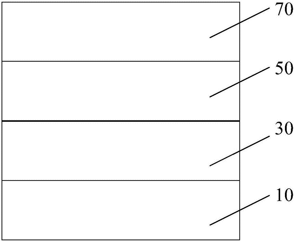
[0078] 2) Fabricate the first carrier injection layer.

[0079] In an air environment, spin-coat PEDOT:PSS (polystyrene sulfonic acid solution) on a clean ITO transparent conductive glass at a speed of 3000 rpm for 45 seconds. After the spin coating is completed, it is annealed at 140° C. for 30 minutes in the air. Then transfer it to a glove box in a nitrogen atmosphere, anneal at 100°C for 40 minutes, and finally form a PEDOT:PSS layer on the surface of ITO, that is, form the first carrier injection l...

Embodiment 2

[0091] The difference between the preparation method provided by this embodiment and Example 1 is:

[0092] Step 3) In the step of making the first carrier transport layer, the synthesized inorganic semiconductor nanocrystal is ZnO nanocrystal, and its specific synthesis method is: 3mmol zinc acetate dihydrate and 30ml DMSO (dimethyl sulfoxide) Add it into a 100ml three-necked flask, heat it in a water bath at 30°C and stir it magnetically. Take another small beaker, add 5mmol TMAH (tetramethylammonium hydroxide) and 10ml ethanol, shake well and mix well, and then seal it with a sealing film; add solution B dropwise to solution A, then continue magnetic stirring, at 30 ° C under a water bath environment and stirred for 1 hour to form inorganic semiconductor nanocrystal ZnO, and then purify the inorganic semiconductor nanocrystal ZnO.

[0093] After the inorganic semiconductor nanocrystal ZnO after above-mentioned purification is made into the normal hexane solution of 10mg / ml...

Embodiment 3

[0096] The difference between the preparation method provided by this embodiment and Example 1 is:

[0097] The molar ratio of the inorganic semiconductor nanocrystals to the chelating agent is 10:1, that is, the above-mentioned inorganic semiconductor nanocrystals NiO are made into a 10 mg / ml n-hexane solution and then 0.5 mmol of the chelating agent is added.


PUM

PropertyMeasurementUnit
Thicknessaaaaaaaaaa

Abstract

The invention provides an inorganic metal compound, a composition comprising the inorganic metal compound, a device, apparatuses, and a manufacturing method for the device. The inorganic metal compound is used for a first current carrier transport layer of a photoelectric device; the inorganic metal compound is a chelate which is obtained from inorganic semiconductor nanocrystals and a chelating agent through a chelating reaction; and first current carriers comprise electrons or holes. By adoption of the inorganic metal compound, material stability can be improved; the chelate with a stable structure is formed by virtue of matching of the chelating agent and active sites of the inorganic semiconductor nanocrystals in the chelating reaction; therefore, by lowering or inactivating the activity of the active sites on the surfaces of the inorganic semiconductor nanocrystals, the capability of accepting external electrons or holes of the active sites is lowered; the electrons or holes of a quantum dot light emitting layer cannot be extracted by the active sites easily; fluorescence quenching of the quantum dots is reduced; the problem of fluorescence quenching of a quantum dot light emitting screen easily caused by the existing inorganic current carrier transport material can be solved; and the light emitting efficiency of the photoelectric device is improved.

Description

technical field [0001] The invention relates to the technical field of light-emitting devices, in particular to an inorganic metal compound, a composition containing it, a device and a device, and a manufacturing method. Background technique [0002] In Quantum Dot Light-Emitting Diode (QLED for short), in order to balance the injection of electrons and holes, a carrier transport layer is usually introduced into the device to speed up the rate of charge transport and injection, for example A hole transport layer is added to accelerate the hole transport rate. Commonly used materials for forming carrier transport layers include organic carrier transport materials and inorganic carrier transport materials, because organic carrier transport layers such as polyvinylcarbazole (PVK) are sensitive and unstable to the environment, It is not suitable for production and application, so more stable inorganic carrier transport materials are generally used, such as inorganic metal compo...

Claims


Application Information

Patent Timeline
IPC IPC(8): H01L51/50H01L51/54H01L51/56H01L27/32
CPCH10K59/00H10K50/14H10K50/15H10K50/16H10K71/00
Inventor 谢松均
Owner NANJING TECH CORP LTD
Why Eureka
Try Eureka