Monocrystalline silicon growth furnace
A growth furnace and monocrystalline silicon technology, applied in the direction of single crystal growth, single crystal growth, crystal growth, etc., can solve the unfavorable furnace temperature field uniformity, oxygen content, lower crystal ingot quality and production cost, unfavorable crystal ingot out of the furnace and cleaning problems to achieve the effect of shortening the melting time, reducing the radial temperature gradient and saving costs
- Summary
- Abstract
- Description
- Claims
- Application Information
AI Technical Summary
Problems solved by technology
Method used
Image
Examples
Embodiment 1
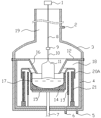
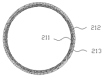
[0049] 8-inch single crystal silicon for N-type integrated circuits is grown by Cz method or magnetic field Cz method, and a 24-inch quartz crucible is used, and the polysilicon raw material loading capacity is 120Kg. The thickness of the diversion guide cylinder is 10mm, and the thermal conductivity of the graphite material used is 20W / m / K; the total thickness of the vertical distributor cylinder is 80mm, and the horizontal distance between the vertical distributor cylinder and the diversion guide cylinder is 20mm , The maximum vertical distance is 100mm, and the bottom of the inner and outer chambers separated by the bottom guide tube are respectively provided with two sets of exhaust valves. The thickness of the quartz tube of the outer layer of the vertical split tube is 20mm, the thickness of the graphite tube of the inner layer is 30mm, and the middle layer is filled with graphite carbon felt.
[0050] After the charging is completed, place the diversion guide tube, clos...
Embodiment 2
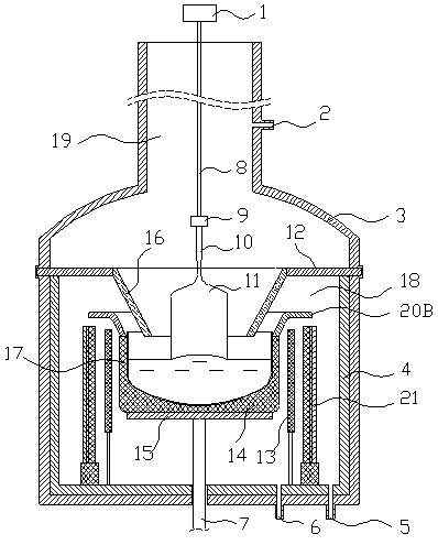
[0053] 8-inch single crystal silicon for N-type integrated circuits is grown by Cz method or magnetic field Cz method, and a 24-inch quartz crucible is used, and the polysilicon raw material loading capacity is 120Kg. The thickness of the diversion guide cylinder is 10mm, and the thermal conductivity of the graphite material used is 20W / m / K; the total thickness of the vertical distributor cylinder is 80mm, and the horizontal distance between the vertical distributor cylinder and the diversion guide cylinder is 20mm , The maximum vertical distance is 100mm, and the bottom of the inner and outer chambers separated by the bottom guide tube are respectively provided with two sets of exhaust valves. The thickness of the quartz tube of the outer layer of the vertical split tube is 20mm, the thickness of the graphite tube of the inner layer is 30mm, and the middle layer is filled with graphite carbon felt.
[0054] After the charging is completed, place the diversion guide tube, clos...
Embodiment 3
[0057] 8-inch single crystal silicon for N-type integrated circuits is grown by Cz method or magnetic field Cz method, and a 24-inch quartz crucible is used, and the polysilicon raw material loading capacity is 120Kg. The thickness of the diversion guide cylinder is 10mm, and the thermal conductivity of the graphite material used is 20W / m / K; the total thickness of the vertical distributor cylinder is 80mm, and the horizontal distance between the vertical distributor cylinder and the diversion guide cylinder is 20mm , The maximum vertical distance is 100mm, and the bottom of the inner and outer chambers separated by the bottom guide tube are respectively provided with two sets of exhaust valves. The thickness of the quartz tube of the outer layer of the vertical split tube is 20mm, the thickness of the graphite tube of the inner layer is 30mm, and the middle layer is filled with graphite carbon felt.
[0058] After the charging is completed, place the diversion guide tube, clos...
PUM
| Property | Measurement | Unit |
|---|---|---|
| thickness | aaaaa | aaaaa |
| height | aaaaa | aaaaa |
| thickness | aaaaa | aaaaa |
Abstract
Description
Claims
Application Information


