Cleaning method for removing metal pollution or residuals of SiC epitaxial wafer

A technology of epitaxial wafers and metals, applied in the direction of electrical components, semiconductor/solid-state device manufacturing, circuits, etc., can solve the problems of reducing breakdown voltage, shortening the lifetime of minority carriers, affecting the reliability of semiconductor device performance, and device yield, so as to prevent Secondary contamination, reduction of re-contamination by metals, and prevention of adsorption of secondary pollutants

Active Publication Date: 2017-06-30
DONGGUAN TIANYU SEMICON TECH
View PDF5 Cites 13 Cited by
  • Summary
  • Abstract
  • Description
  • Claims
  • Application Information

AI Technical Summary

Problems solved by technology

[0007] During the manufacturing process of semiconductor devices, the cleanliness of semiconductor materials has an important impact on the performance and yield of the devices, while metal contamination or residues will shorten the minority carrier lifetime, reduce the breakdown voltage and other consequences, affecting the reliability and performance of semiconductor devices. Device Yield

Method used


Image

  • Cleaning method for removing metal pollution or residuals of SiC epitaxial wafer
  • Cleaning method for removing metal pollution or residuals of SiC epitaxial wafer
  • Cleaning method for removing metal pollution or residuals of SiC epitaxial wafer

Examples


Embodiment 1

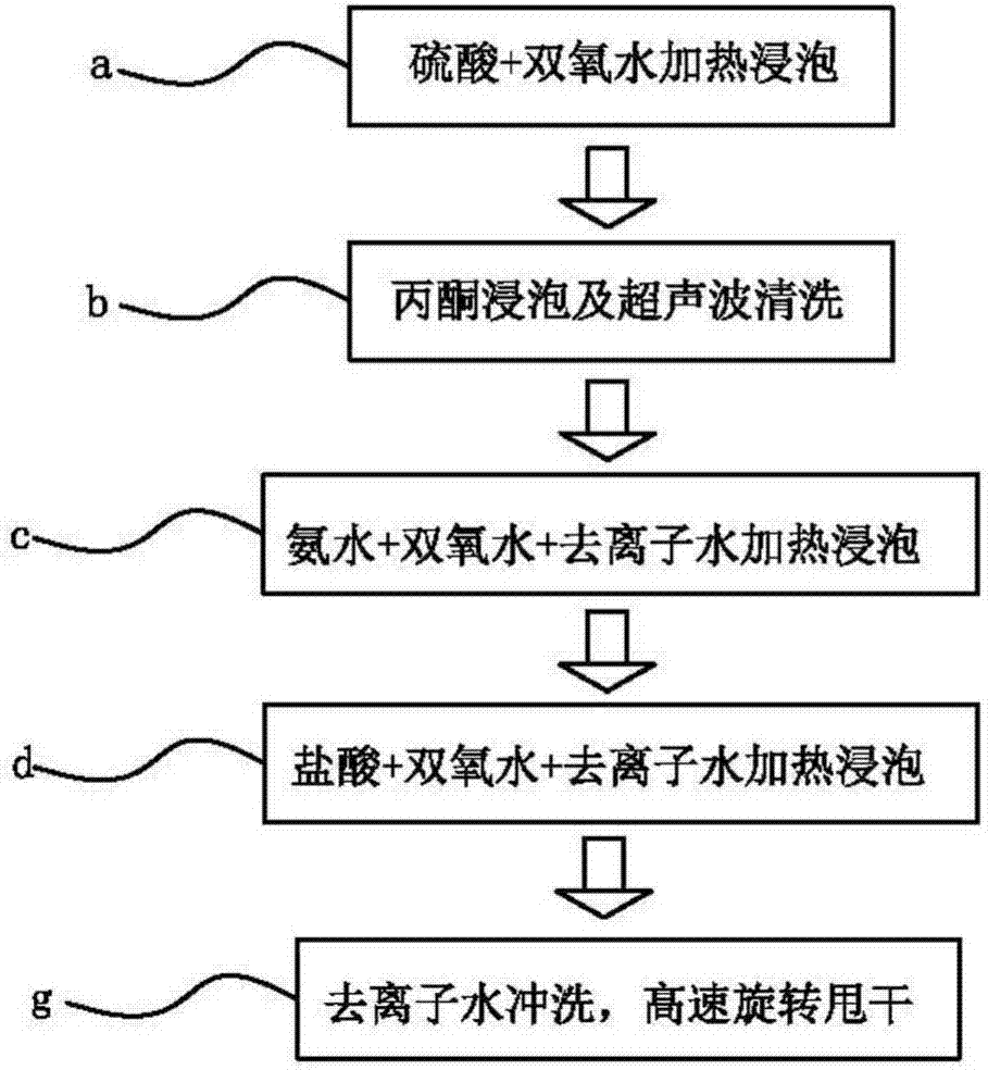
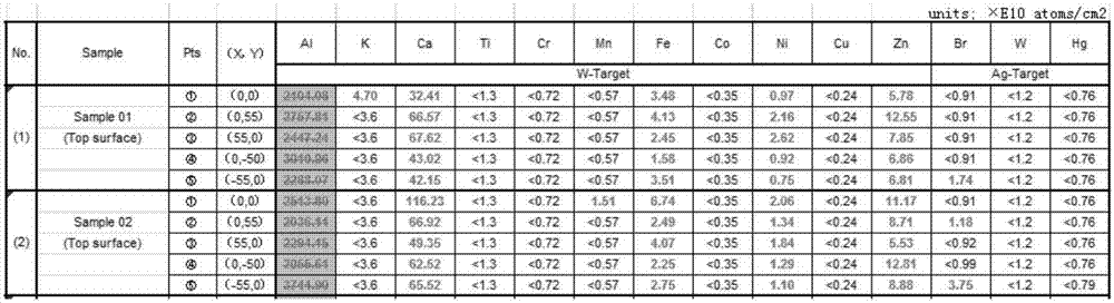
[0042] combine figure 1 As shown, this embodiment one uses steps a, b, c, d, and g in the above-mentioned cleaning method for removing metal contamination or residues on SiC epitaxial wafers, and the test results of two samples in this embodiment one show: Calcium (Ca) residue The minimum value is 3.241E+11atom / cm 2 , the maximum value is 1.1623E+12atom / cm 2 ; The minimum iron (Fe) residue is 1.58E+10atom / cm 2 , the maximum value is 6.74E+10atom / cm 2 ; The minimum zinc (Zn) residue is 5.53E+10atom / cm 2 , the maximum value is 1.281E+11atom / cm 2 ;The residual content of other metal elements is less than 5E+10atom / cm 2 , see the test value image 3 .

Embodiment 2

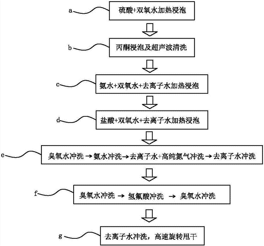
[0044] combine figure 2 As shown, the present embodiment 2 uses steps a, b, c, d, e, f, and g in the above-mentioned cleaning method for removing metal contamination or residue on SiC epitaxial wafers. The test results of the two samples in the present embodiment 2 show: the sample 04 (Sample 04) The content of potassium (K) and calcium (Ca) in the central point is relatively high, and the other test points are all less than 5E+10atom / cm 2 ; The minimum iron (Fe) residue is less than 0.45E+10atom / cm 2 , the maximum value is 0.88E+10atom / cm 2 ; The minimum residual amount of zinc (Zn) is less than 0.21E+10atom / cm 2 , the maximum value is 1.41E+10atom / cm 2 ;The residual content of other metal elements is less than 2E+10atom / cm 2 , see the test value Figure 4 .

[0045] Embodiment 2 has a better effect of removing metal pollution or residue, and the result meets the material requirements of the semiconductor industry.


PUM


Abstract

The invention discloses a cleaning method for removing metal pollution or residuals of a SiC epitaxial wafer, and the method comprises the following steps: a, putting the SiC epitaxial wafer in mixed washing liquor, formed by the mixing of sulfuric acid and hydrogen peroxide, for immersing; b, cleaning the surface of the SiC epitaxial wafer through deionized water, and then putting the SiC epitaxial wafer in acetone for ultrasonic cleaning; c, cleaning the surface of the SiC epitaxial wafer through deionized water, and then putting the SiC epitaxial wafer in heated mixed washing liquor, formed by the mixing of ammonia water, hydrogen peroxide and deionized water, for immersing; d, , cleaning the surface of the SiC epitaxial wafer through deionized water, and then putting the SiC epitaxial wafer in heated mixed washing liquor, formed by the mixing of hydrochloric acid, hydrogen peroxide and deionized water, for immersing; e, sequentially cleaning the surface of the SiC epitaxial wafer through ozone water, ammonia water, high-purity nitrogen and deionized water; f, sequentially cleaning the surface of the SiC epitaxial wafer through ozone water, hydrofluoric acid liquor and ozone water; g, cleaning the surface of the SiC epitaxial wafer through deionized water, and rotating the SiC epitaxial wafer at a high speed for drying.

Description

[0001] Technical field: [0002] The invention relates to the technical field of semiconductors, in particular to a cleaning method for removing metal pollution or residues on SiC epitaxial wafers. [0003] Background technique: [0004] Silicon carbide (SiC) is an important wide-bandgap semiconductor material. SiC is a new generation (third-generation) wide-bandgap semiconductor material with excellent performance. It is a typical representative of the third-generation semiconductor material. It is one of the wide-bandgap semiconductor materials with the most mature technology and device manufacturing level and the most widely used. It is an ideal semiconductor material for high-temperature, high-frequency, radiation-resistant, and high-power applications. SiC semiconductor materials have outstanding advantages such as wide band gap, high saturation drift velocity, high thermal conductivity, and high critical breakdown electric field, and are especially suitable for making hig...

Claims


Application Information

Patent Timeline
Patent Type & Authority Applications(China)
IPC IPC(8): H01L21/02H01L21/311
CPCH01L21/02068H01L21/31111
Inventor 刘丹孙国胜孔令沂张新河韩景瑞李锡光萧黎鑫
Owner DONGGUAN TIANYU SEMICON TECH
Why Eureka
Try Eureka