Micro-fluidic chip manufacturing method based on nanofiber template method

A microfluidic chip and nanofiber technology, applied in chemical instruments and methods, laboratory containers, laboratory utensils, etc., can solve the problems of high molding pressure, low machining surface accuracy, long heating time, etc. The effect of high molding precision

Active Publication Date: 2017-07-07
BEIJING UNIV OF CHEM TECH
View PDF4 Cites 5 Cited by
  • Summary
  • Abstract
  • Description
  • Claims
  • Application Information

AI Technical Summary

Problems solved by technology

[0003] Traditional microfluidic chip microchannel molding processing is mainly injection molding and thermocompression molding, such as Chinese patents 201110072477.7, 201010119177.5, 200910308065.1, 201010300409.7, which provide various microfluidic chip injection molds with microchannel structures on the molding surface, However, due to the micro-scale effect, there are problems of difficult filling and molding of micro-channels, and the manufacturing of injection molds for microfluidic chips is difficult, the injection molding process is complicated, and the production cost is high; thermocompression molding has long heating time, high energy consumption, and high production costs. Problems such as high pressure, thermal deformation and limited f

Method used


Image

  • Micro-fluidic chip manufacturing method based on nanofiber template method
  • Micro-fluidic chip manufacturing method based on nanofiber template method
  • Micro-fluidic chip manufacturing method based on nanofiber template method

Examples


Example Embodiment

[0022] Example 1

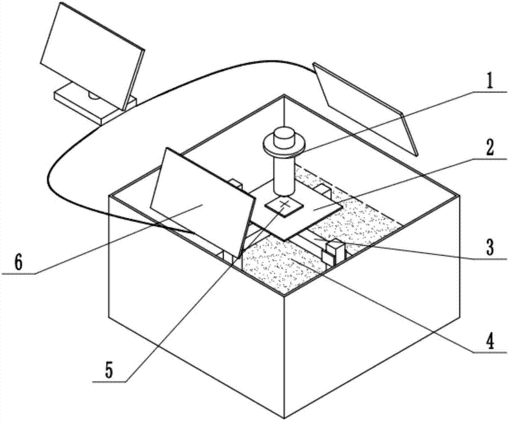
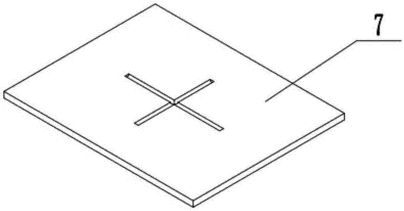
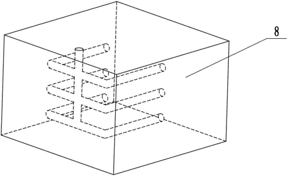
[0023] The present invention proposes a method for manufacturing a microfluidic chip based on the nanofiber template method. The method includes: first placing a receiving plate 2 on a three-dimensional motion platform 3, following the motion platform 3 for three-dimensional motion, and placing the motion platform 3 and the receiving plate 2 on the mounting plate. In the container with the liquid light-curing material 4, make the liquid light-curing material 4 pass the receiving plate 2 for a certain distance, and turn on the surface light sources 6 distributed on both sides of the spinning nozzle 1 to solidify the liquid light-curing material above the receiving plate 2 , Forming a microfluidic chip substrate. The soluble polymer solution / melt is passed through the spinning nozzle 1 for near-field electrospinning or microflow spinning, and the order of the fibers on the receiving plate 2 is achieved by controlling the relationship between the falling speed of ...

Example Embodiment

[0025] Example 2

[0026] Spread a layer of acrylic resin on the receiving plate 2 as the light-curing material 4, and use this as the spinning receiving plate 2 to be placed on the moving platform 3, following the moving platform 3 for three-dimensional movement, the moving platform 3 and the receiving plate 2 are placed In a container filled with acrylic resin, make the liquid light-curing material 4 cover the receiving plate 2 for a certain distance, and turn on the surface light sources 6 distributed on both sides of the spinning nozzle 1 to cure the liquid light-curing material above the receiving plate 2 , To form a microfluidic chip substrate; add PEG pellets to the polymer melt spinning nozzle 1, heat the temperature to 60°C to melt and plasticize, adjust the distance between the spinning nozzle 1 and the receiving plate 2 to 5mm , The spinning voltage is 1kV, and the near-field melt electrospinning is started; the moving speed of the moving platform 3 is adjusted to 310m...


PUM


Abstract

The invention discloses a micro-fluidic chip manufacturing method based on the nanofiber template method. Firstly, a receiving plate is coated with a photo-curing material layer to form a micro-fluidic chip substrate; secondly, near-field electrospinning or micro liquid spinning is conducted to obtain a first fiber layer with a certain pattern; thirdly, the receiving plate descends by a certain height along with a moving platform, orderly sedimentation of a second fiber layer is conducted, and spinning and curing are conducted layer by layer to obtain a photo-curing model combining orderly fibers with a photo-curing material; fourthly, a last fiber layer is communicated with the surface of the photo-curing model, and when the fibers are completely wrapped by the photo-curing material and certain allowance is reserved, forming of the photo-curing model is completed; fifthly, the photo-curing model is taken out and placed into a solvent, and ultrasonic shaking soluble fibers are added; sixthly, when micro-nanofibers are completely dissolved, the model is taken out to obtain a micro-fluidic chip. The soluble fibers serve as channel filler, and forming precision can reach the precision level same as that of the fiber diameter.

Description

technical field [0001] The invention relates to a method for manufacturing a microfluidic chip by using a nanofiber template, in particular to a method for manufacturing a microfluidic chip with nano-channels or complex three-dimensional channels, and belongs to the technical field of micro-nano processing. Background technique [0002] Microfluidic chips are based on the basic principles and technologies of ordinary capillary electrophoresis, and use micro-nano processing technology to process various microstructures on silicon, quartz, glass or polymer matrix materials, such as pipes and reaction pools. , electrodes and other functional units to complete a series of tasks involved in the fields of biology and chemistry, such as sample preparation, biochemical reactions, processing (mixing, filtration, dilution), separation and detection, etc., with fast, efficient, low consumption, and analysis process A miniature analytical experimental device with the characteristics of ...

Claims


Application Information

Patent Timeline
IPC IPC(8): B01L3/00
CPCB01L3/502707B01L2300/08B01L2300/12
Inventor 李好义李轶杨卫民丁玉梅谭晶程礼盛
Owner BEIJING UNIV OF CHEM TECH
Why Eureka
Try Eureka