Texturing method of diamond wire slice polycrystalline black silicon

A diamond wire and slicing technology, which is applied in the field of solar cells, can solve the problems of high cost, complicated process, and difficulty in control, and achieve the effects of reasonable sequence, improved short-circuit current reflectivity, and small efficiency attenuation

Active Publication Date: 2017-07-07
江苏福吉食品有限公司
View PDF5 Cites 18 Cited by
  • Summary
  • Abstract
  • Description
  • Claims
  • Application Information

AI Technical Summary

Problems solved by technology

There are dry etching and wet etching methods to realize polycrystalline black silicon texture. Among them, dry etching is mainly represented by reactive ion etching. The process is extremely co

Method used


Image

  • Texturing method of diamond wire slice polycrystalline black silicon
  • Texturing method of diamond wire slice polycrystalline black silicon
  • Texturing method of diamond wire slice polycrystalline black silicon

Examples


Embodiment 1

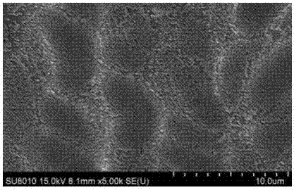
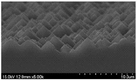
[0045] A method for making texture of polycrystalline black silicon sliced ​​by diamond wire, which comprises the following steps in sequence: 1) pretreating the silicon wafer in a solution containing nitric acid and hydrofluoric acid; 2) placing the pretreated silicon wafer in a solution containing Pre-deposition of oxidized metal nanoparticles in a metal salt solution; 3) depositing oxidized metal particles by placing the pre-deposited silicon wafer in a solution containing hydrofluoric acid and an oxidizing agent; 4) depositing the deposited silicon wafer Place in a solution containing hydrofluoric acid, oxidant, and metal salt ions for longitudinal and transverse hole expansion corrosion; 5) place the expanded silicon wafer in an acid solution to remove metal ions; 6) remove metal ions from the silicon wafer The final texture is formed by placing it in a solution containing a texture additive for modification of the nanostructure.

[0046] In this embodiment, the molar con...

Embodiment 2

[0048] In Example 2, the molar concentration of hydrofluoric acid in step 1) is 10 mol / L, and the molar concentration of nitric acid is 10 mol / L. In step 2, the metal salt is copper nitrate and silver nitrate, the molar concentration of the metal salt is 0.000001mol / L~2.5mol / L, the pre-deposition temperature is 60°C, and the pre-deposition time is 900 seconds. The molar concentration of hydrofluoric acid is 10mol / L in the step 3, and oxygenant is H 2 o 2 、HNO 3 solution, the molar concentration of the oxidizing agent is 10mol / L, the deposition temperature is 60°C, and the reaction time is 900 seconds; the molar concentration of hydrofluoric acid in step 4 is 10mol / L, and the oxidizing agent is H 2 o 2 、HNO 3 Solution, the molar concentration of the oxidant is 10mol / L, the metal salt ions are silver ions and copper ions, the molar concentration of the metal salt ions is 2.5mol / L, the reaction temperature is 60°C, and the reaction time is 900 seconds. In step 5, the acid so...

Embodiment 3

[0050] In embodiment 3, the molar concentration of hydrofluoric acid in step 1 is 6mol / L, and the molar concentration of nitric acid is 6mol / L. In step 2, the metal salts are copper nitrate and silver nitrate, the molar concentration of the metal salts is 2 mol / L, the pre-deposition temperature is 40° C., and the pre-deposition time is 120 seconds. The molar concentration of hydrofluoric acid is 6mol / L in the step 3, and oxygenant is H 2 o 2 、HNO 3 solution, the molar concentration of the oxidizing agent is 5mol / L, the deposition temperature is 40°C, and the reaction time is 120 seconds; the molar concentration of hydrofluoric acid in step 4 is 6mol / L, and the oxidizing agent is H 2 o 2 solution, the molar concentration of the oxidant is 6mol / L, the metal salt ions are silver ions and copper ions, the molar concentration of the metal salt ions is 2mol / L, the reaction temperature is 40°C, and the reaction time is 120 seconds. In step 5, the acid solution is nitric acid, the...


PUM


Abstract

The invention discloses a texturing method of diamond wire slice polycrystalline black silicon. The texturing method comprises the following steps in turn: a silicon chip is arranged in a solution containing nitric acid and hydrofluoric acid to be preprocessed; the preprocessed silicon chip is arranged in a solution containing metal salt to perform pre-deposition of oxidized metal nanoparticles; the silicon chip after pre-deposition is arranged in a solution containing hydrofluoric acid and an oxidizing agent to perform deposition of the oxidized metal nanoparticles; the silicon chip after deposition is arranged in a solution containing hydrofluoric acid, the oxidizing agent and metal salt ions to perform longitudinal and transverse broaching corrosion; the silicon chip after broaching is arranged in an acid solution to remove the metal ions; and the silicon chip of which the metal ions are removed is arranged in an alkaline solution containing a texturing additive to perform modification of the nanostructure so as to form the final textured surface. The non-uniformity and the chromatic aberration of the appearance after texturing can be effectively avoided.

Description

technical field [0001] The invention relates to the technical field of solar cells, in particular to a texturing method for diamond wire sliced ​​polycrystalline black silicon. Background technique [0002] Solar power generation is an important part of the new energy field. Silicon wafers account for the largest proportion of the cost structure of crystalline silicon solar cells, and reducing the cost of silicon wafers is crucial to achieving grid parity for photovoltaics. Diamond wire cutting silicon wafer is a new technology developed in recent years. Compared with the traditional mortar slicing process, it has the advantages of less silicon consumption per unit capacity, high slicing efficiency, low cost of auxiliary materials, and thin silicon wafers can be sliced. Due to the popularization of diamond wire slicing technology at the silicon wafer end, the cost of monocrystalline silicon solar cells has dropped rapidly. [0003] Therefore, it is particularly urgent for ...

Claims


Application Information

Patent Timeline
IPC IPC(8): H01L31/0236C30B33/10H01L31/18
CPCC30B33/10H01L31/02363H01L31/1804Y02P70/50
Inventor 黄锦锋
Owner 江苏福吉食品有限公司
Why Eureka
Try Eureka