
Production method of replacement embedded copper block of circuit board

A production method and circuit board technology, applied in the directions of printed circuit manufacturing, printed circuits, printed circuits, etc., can solve the problems of high scrap rate, layered explosion, low production efficiency, etc., to reduce production costs, excellent heat dissipation performance, The effect of improving production efficiency

Active Publication Date: 2017-07-18
SHENZHEN SUNTAK MULTILAYER PCB
View PDF3 Cites 11 Cited by
  • Summary
  • Abstract
  • Description
  • Claims
  • Application Information

AI Technical Summary

Problems solved by technology

[0007] The present invention aims at the problems of embedding high thermal conductivity metal copper blocks or other metal blocks in the existing high heat dissipation circuit boards for heat dissipation, resulting in inability to batch production, low production efficiency, high scrap rate and high production cost, and provides a circuit board Substituting the production method of buried copper blocks, this method provides a technical solution for embedding high thermal conductivity metal copper blocks or metal blocks in circuit boards, and solves the problems of poor reliability and delamination of circuit boards caused by filling metal block products ; And it can be mass-produced, which improves the production efficiency of the circuit board, reduces the scrap rate and thus reduces the production cost, and at the same time can ensure the excellent heat dissipation performance of the product

Method used


Image

  • Production method of replacement embedded copper block of circuit board
  • Production method of replacement embedded copper block of circuit board

Examples


Embodiment

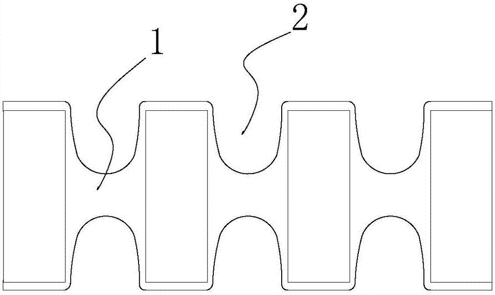
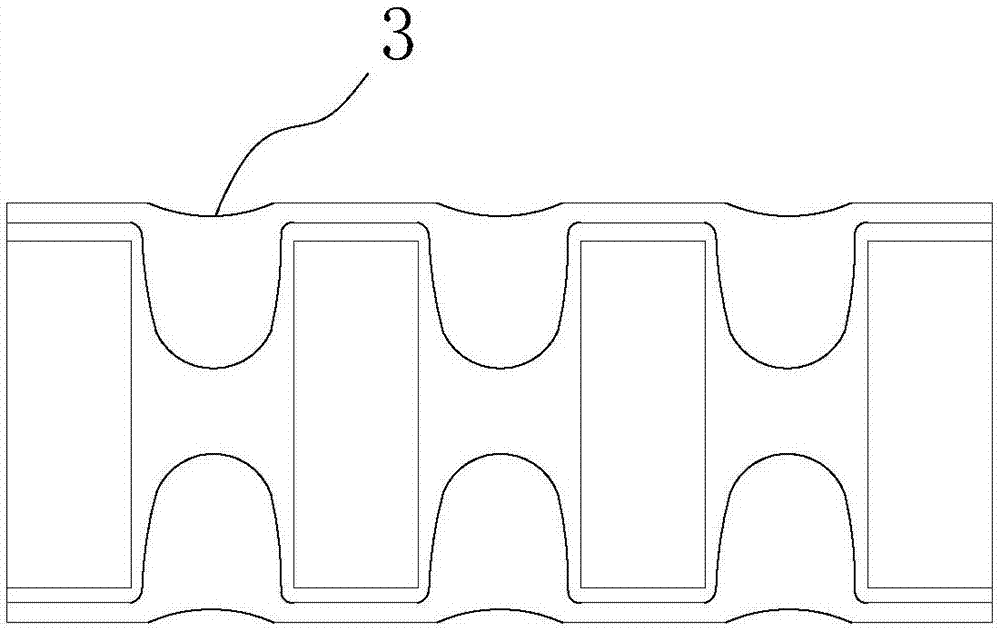
[0028] like figure 1 and figure 2 As shown, a manufacturing method for replacing buried copper blocks in circuit boards shown in this embodiment includes the following processing steps in sequence: material cutting→making inner layer circuits→pressing→drilling target holes→drilling→plasma treatment→sinking Copper 1→full board electroplating 1→pulse electroplating bridging→full board hole filling electroplating→outer layer drilling→immersion copper 2→full board electroplating 2→making outer layer lines and copper pillars→solder mask→silk printing characters→surface treatment→forming ,Specific steps are as follows:

[0029] a. Cutting: cut out the core board according to the panel size 520mm×620mm, and the thickness of the core board is 1.2mm H / H;

[0030] b. Making the inner layer circuit (negative film process): the inner layer pattern is transferred, and the photosensitive film is coated with a vertical coating machine. The film thickness of the photosensitive film is cont...


PUM


Abstract

The invention discloses a production method of a replacement embedded copper block of a circuit board. The production method comprises steps that a target hole is drilled in a production board after early stage stitching, and a through hole is drilled in the position of the target hole; glue refuses on the production board are removed by adopting plasma glue removing operation, and the through hole is metalized by adopting an electroless plating copper and full board electroplating operation; the copper (electro)plating bridging of the middle position of the metalized through hole is carried out by adopting an pulse plating bridging operation, and then a double-sided blind hole is formed; the copper (electro)plating is carried out in the double-sided blind hole to fill and level up the double-sided blind hole by adopting a full board filling electroplating operation; the circuit board is produced by sequentially carrying out the drilling operation, the electroless plating copper operation, the full board electroplating operation, and other latter operations on the production board. A metal copper block is formed on the production board in an electroplated way to replace a conventional high heat conduction metal copper block or a metal block embedded in the circuit board, and the problems of the circuit board such as poor reliability and delamination and blistering caused by the filling of the metal block product are solved, and therefore the production efficiency of the circuit board, a rejection rate is reduced, and the excellent heat dissipation performance of the product is guaranteed.

Description

technical field [0001] The invention relates to the technical field of printed circuit board production, in particular to a production method for replacing buried copper blocks in circuit boards. Background technique [0002] With the rapid development of electronic products in the direction of light, thin, small, high density, and multi-function, the volume of electronic components and logic circuits has been reduced exponentially, while the operating frequency has increased sharply and power consumption has continued to increase, resulting in the working environment of components. Changes in the direction of high temperature have put forward higher and higher requirements for the heat dissipation of PCB products. If there is no good heat dissipation method to eliminate the heat generated by electrons, these excessively high temperatures will cause electronic components to generate electron ionization and thermal stress. Resulting in reduced overall stability and shortened ...

Claims


Application Information

Patent Timeline
Patent Type & Authority Applications(China)
IPC IPC(8): H05K3/42
CPCH05K3/423H05K2201/09509
Inventor 周文涛杨辉腾李永妮翟青霞黄宏波宋清
Owner SHENZHEN SUNTAK MULTILAYER PCB
Learn More