
Thin film assembled by gold nanoparticles and its preparation method and use

A technology of gold nanoparticles and thin films, which is applied in the field of thin films assembled by gold nanoparticles and its preparation, can solve the problems of affecting the uniformity of SERS signals, restricting SERS activity, and high SERS activity, so as to reduce the interference of background signals and achieve high SERS Activity, activity-enhancing effect

Active Publication Date: 2019-04-05
HEFEI INSTITUTES OF PHYSICAL SCIENCE - CHINESE ACAD OF SCI
View PDF2 Cites 2 Cited by
  • Summary
  • Abstract
  • Description
  • Claims
  • Application Information

AI Technical Summary

Problems solved by technology

Although this product has strong light absorption at 633nm and 785nm, it has disadvantages with its preparation method. First, the gold nanoparticles in the product are only a single layer, which not only restricts its SERS activity, but also The uniformity is also very easy to be destroyed by the water waiting for the test solution, thereby seriously affecting the uniformity of its SERS signal; secondly, the preparation method cannot obtain a product with high SERS activity and is not subject to the water waiting for the test solution to destroy the uniformity of its SERS signal

Method used


Image

  • Thin film assembled by gold nanoparticles and its preparation method and use
  • Thin film assembled by gold nanoparticles and its preparation method and use

Examples


Embodiment 1

[0037] The concrete steps of preparation are:

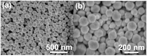
[0038] After first cleaning the conductive substrate with ethanol and deionized water, sputter a 10nm thick gold film on the surface of the conductive substrate; wherein the conductive substrate is an indium tin oxide glass substrate, and obtain a conductive substrate covered with a gold film on its surface. end. Then put the graphite sheet as the anode and the conductive substrate covered with gold film as the cathode in the gold electrolyte, at 20μA / cm 2 After electrodeposition at a constant current for 120 minutes, it was washed once with deionized water, and then dried at 40°C; the gold electrolyte was 0.2 g / L chloroauric acid aqueous solution and 200 g / L polyvinylpyrrolidone aqueous solution The mixed solution, wherein the polyvinylpyrrolidone its molecular weight is 40000 polyvinylpyrrolidone, made approximately figure 1 A thin film assembled with gold nanoparticles is shown.

Embodiment 2

[0040] The concrete steps of preparation are:

[0041] After first cleaning the conductive substrate with ethanol and deionized water, sputter a 15nm thick gold film on the surface of the conductive substrate; wherein the conductive substrate is an indium tin oxide glass substrate, and obtain a conductive substrate covered with a gold film on its surface. end. Then put the graphite sheet as the anode and the conductive substrate covered with gold film as the cathode in the gold electrolyte, at 140μA / cm 2 After electrodeposition at a constant current for 95 minutes, it was washed twice with deionized water, and then dried at 45°C; the gold electrolyte was 2.5g / L chloroauric acid aqueous solution and 150g / L polyvinylpyrrolidone aqueous solution The mixed solution, wherein the polyvinylpyrrolidone its molecular weight is 40000 polyvinylpyrrolidone, made approximately figure 1 A thin film assembled with gold nanoparticles is shown.

Embodiment 3

[0043] The concrete steps of preparation are:

[0044]After first cleaning the conductive substrate with ethanol and deionized water, sputter a 20nm thick gold film on the surface of the conductive substrate; wherein the conductive substrate is an indium tin oxide glass substrate, and obtain a conductive substrate covered with a gold film on its surface. end. Then the graphite sheet is used as the anode, and the conductive substrate covered with gold film on the surface is used as the cathode, placed in the gold electrolyte, at 260μA / cm 2 After electrodeposition at a constant current for 70 minutes, it was washed twice with deionized water, and then dried at 50°C; wherein, the gold electrolyte was a mixture of 5 g / L chloroauric acid aqueous solution and 100 g / L polyvinylpyrrolidone aqueous solution. Mixed solution, polyvinylpyrrolidone wherein its molecular weight is the polyvinylpyrrolidone of 40000, makes as figure 1 A thin film assembled with gold nanoparticles is shown. ...


PUM

PropertyMeasurementUnit
thicknessaaaaaaaaaa
particle diameteraaaaaaaaaa
wavelengthaaaaaaaaaa

Abstract

The invention discloses a film assembled from gold nanoparticle, as well as a preparation method and application of the film. A plurality of layers of the gold nanoparticles are mutually adhered on a conducting substrate so as to form the film of which the thickness is 200nm-2<mu>m, wherein the grain diameter of the gold nanoparticles is 30-120nm; and the clearance or gap between every two gold nanoparticles is equal to or smaller than 10nm. The method comprises the following steps of: sputtering a gold film on the surface of the conducting substrate so as to obtain the conducting substrate of which the surface is covered with the gold film; placing the conducting substrate in gold electrolyte by using a graphite flake as anode and using the conducting substrate of which the surface is covered with the gold film as a cathode; and performing electro-deposition under constant current to obtain the target product. The film is high in SERS activity, and is extremely easy to widely and commercially apply to rapid trace detection for parathion-methyl of pesticides.

Description

technical field [0001] The invention relates to a thin film and its preparation method and use, in particular to a thin film assembled with gold nanoparticles and its preparation method and use. Background technique [0002] Due to the resonance properties of surface plasmons, noble metal nanostructures or micro-nanostructures have a wide range of applications in surface-enhanced spectroscopy, especially SERS spectroscopy. Recently, people have made some useful attempts and efforts to obtain noble metal micro-nanostructures with surface plasmon resonance properties, such as "Facile Fabrication of High-DensitySub-1-nm Gaps from Au Nanoparticle Monolayers as Reproducible SERSSubstrates" , Adv.Funct.Mater.2016,26,8137-8145 (“Facile preparation of single-layer gold nanoparticle films with high-density subnanometer gaps as reproducible SERS substrates”, Advanced Functional Materials, Vol. 26, 2016 pp. 8137-8145). The single-layer gold nanoparticle film mentioned in this article...

Claims


Application Information

Patent Timeline
Patent Type & Authority Patents(China)
IPC IPC(8): C23C28/02C23C14/16C23C14/18C23C14/34C25D3/48C25D7/12C25D5/34G01N21/65
CPCC01P2002/82C01P2004/03C23C14/16C23C14/18C23C14/34C23C28/023C25D3/48C25D5/34C25D7/006C25D7/12G01N21/658
Inventor 朱储红孟国文
Owner HEFEI INSTITUTES OF PHYSICAL SCIENCE - CHINESE ACAD OF SCI
Learn More