Process for direct imaging growth of graphene on insulation substrate

A technology of insulating substrate and process method, which is applied in the direction of metal material coating process, gaseous chemical plating, coating, etc., can solve the problems of graphene transfer damage, graphene doping, poor substrate adhesion, etc., to achieve Save process steps and process time, improve adhesion, avoid the effect of doping

Inactive Publication Date: 2017-08-04
BEIJING UNIV OF TECH
View PDF4 Cites 7 Cited by
  • Summary
  • Abstract
  • Description
  • Claims
  • Application Information

AI Technical Summary

Problems solved by technology

[0008] The purpose of the present invention is to provide a process method for directly growing graphene by patterning an insulating substrate, which can simultaneously solve the problems of graphene transfer damage, poor adhesion to the substrate, and doping of graphene by photoresist in the photolithography process.

Method used


Image

  • Process for direct imaging growth of graphene on insulation substrate
  • Process for direct imaging growth of graphene on insulation substrate
  • Process for direct imaging growth of graphene on insulation substrate

Examples


Embodiment 1

[0044] Embodiment 1: applied in the graphene field effect transistor

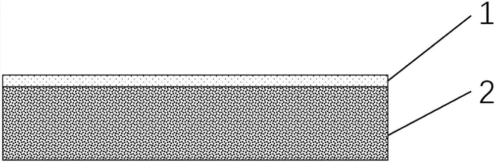
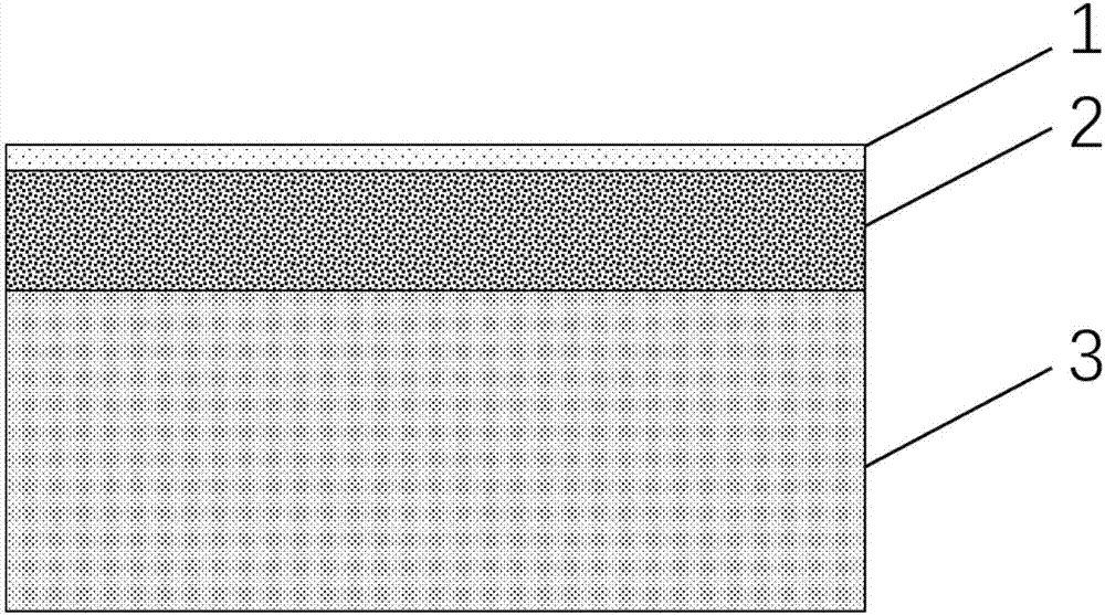
[0045] like Figure 8 As shown, wherein 1 is graphene, 4 is a titanium-platinum electrode, and 5 is a silicon substrate with a 300nm silicon dioxide layer. Graphene field effect transistors were prepared with titanium and platinum as the source and drain electrodes, heavily doped silicon substrates as the gate, and graphene as the conductive channel. The advantage of using titanium-platinum as the electrode is that the titanium-platinum electrode can be prepared in advance, and then graphene can be directly grown by CVD. Titanium-platinum has a high melting point and can withstand the temperature of CVD to directly grow graphene. In this way, after the graphene is grown, the device is finished, so there is no need to prepare electrodes through photolithography-sputtering-stripping, which can minimize the doping of graphene during the device process. Specific steps are as follows:

[0046] S1 After cleani...

Embodiment 2

[0050] Embodiment 2: a graphene field effect transistor using graphite as source and drain electrodes.

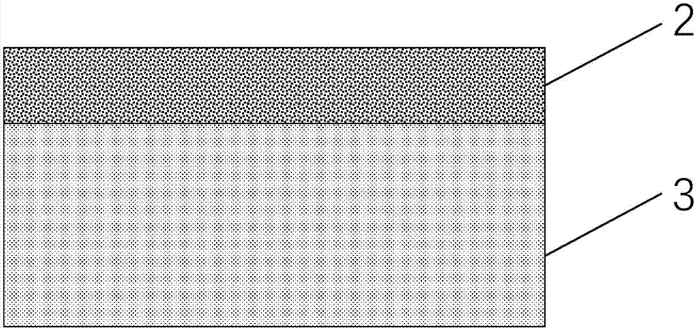
[0051] like Figure 9 As shown, graphite is prepared by CVD method as the source and drain electrodes, the heavily doped silicon substrate is used as the gate, and then graphene is directly grown as the conductive channel to prepare a graphene field effect transistor, in which 1 is graphene and 6 is graphite The electrode, 5, is a silicon substrate with a 300nm silicon dioxide layer. The advantages of using graphite as the source-drain electrode are: 1) Graphite has a very high melting point and can remain stable at the growth temperature of graphene. 2) Graphene and graphite are both carbon materials, and their work functions are similar. Using graphite as an electrode can reduce the contact resistance between graphene and the electrode. 3) Graphite is a carbon material with large reserves in nature, low cost and more environmentally friendly. Specific steps are as foll...

Embodiment 3

[0055] Embodiment 3: using quartz as a substrate to directly grow a graphene film.

[0056] like Figure 10 As shown, the graphene film is directly grown on a quartz substrate, wherein, 1 is graphene, and 7 is a quartz substrate. The main component of quartz is silicon dioxide, which can withstand the temperature of direct growth of graphene. The specific process steps are as follows:

[0057] S1 sputters a layer of 60nm thick copper film on the quartz substrate, such as Figure 10.1 shown.

[0058] S2 uses Black Magic vertical cold wall CVD equipment to prepare graphene at a temperature of 960°C, methane flow rate of 30 sccm, hydrogen gas flow rate of 20 sccm, air pressure of 6 mbar, and growth time of 5 min. A layer of graphene film is grown on the copper film, such as Figure 10.2 shown.

[0059] S3 keeps this temperature and the gas flow constant, and continues annealing to completely volatilize the copper, and the graphene will eventually fall on the quartz substrate,...


PUM

PropertyMeasurementUnit
thicknessaaaaaaaaaa

Abstract

The invention discloses a process for direct imaging growth of graphene on an insulation substrate, and belongs to the field of preparation of graphene materials. The graphene directly grows on the insulation substrate; and the imaging growth of the graphene is performed on the basis. A layer of copper is firstly plated on the insulation substrate as a catalyst; then, the graphene grows on the surface of the plated copper under catalyst of the copper; the high-temperature annealing is kept to volatilize the copper; and after the copper is volatilized, the graphene can fall to the surface of the insulation substrate to achieve the purpose of directly growing the graphene on the insulation substrate. Based on direct growth, the plated copper has a certain patterns through a photolithography process; and correspondingly, the graphene growing on the copper also has the same patterns to achieve the purpose of direct imaging growth of the graphene on the insulation substrate. The process prevents damage of the graphene in a graphene transfer process through the direct growth process, is lower in cost, and is suitable for large-scale batch production of the graphene.

Description

technical field [0001] The invention relates to a novel graphene preparation process, which belongs to the field of graphene material preparation. Background technique [0002] As a new material, graphene has many unique properties, such as: high carrier mobility, high Young's modulus, high light transmittance, etc., and is favored by scientists. At present, its main preparation methods are divided into the following categories: mechanical stripping method, chemical vapor deposition (CVD), redox method, and silicon carbide epitaxy method. Among them, although the quality of graphene prepared by mechanical exfoliation is high, the process is cumbersome, the efficiency is low, and the number of graphene layers is uncontrollable, so it is not suitable for mass production; although the redox method has a high yield, the quality of graphene is poor, and the prepared There are many layers of graphene; although the quality of graphene prepared by silicon carbide epitaxy is high, i...

Claims


Application Information

Patent Timeline
Patent Type & Authority Applications(China)
IPC IPC(8): C23C16/26C23C16/02C23C16/56
CPCC23C16/0281C23C16/26C23C16/56
Inventor 孙捷徐晨董毅博解意洋荀孟潘冠中王秋华
Owner BEIJING UNIV OF TECH
Why Eureka
Try Eureka