A high-power and low-noise planar Gunn diode and its preparation method
A Gunn diode and low-noise technology, applied in the field of diodes in microwave devices, can solve the problems of losing the advantages of two-dimensional integration, large phase noise of devices, and few resonant cavities, achieving small size, reducing phase noise, and improving emission The effect of power
- Summary
- Abstract
- Description
- Claims
- Application Information
AI Technical Summary
Problems solved by technology
Method used
Image
Examples
Embodiment 1
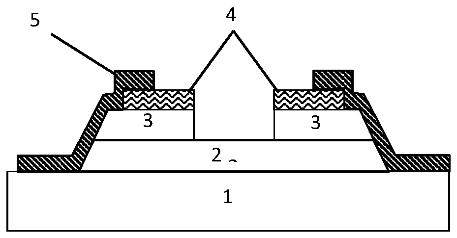
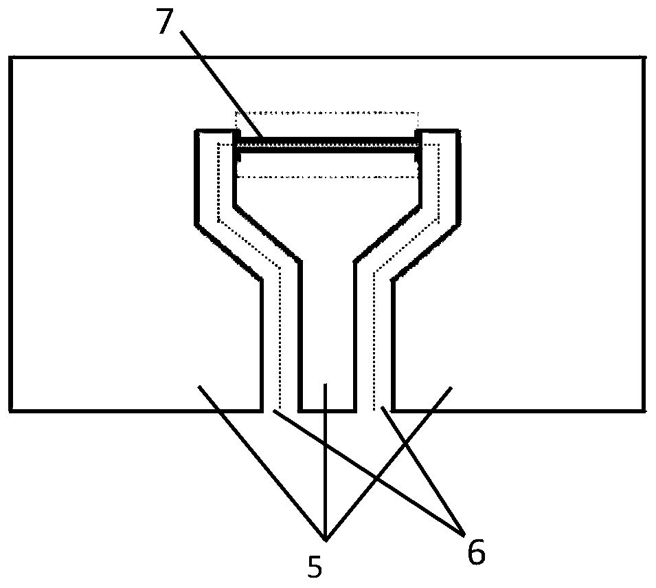
[0043] A high-power and low-noise planar Gunn diode, comprising an insulating substrate 1, a channel layer 2, and a coplanar waveguide 5 arranged on the channel layer 2, the resonant cavity length of the coplanar waveguide 5 is half of the resonance Integer multiples of the wavelength, the characteristic impedance of the coplanar waveguide 5 at the resonant frequency is equal to the load impedance 50Ω.
[0044] The load impedance is 50Ω, and the resonant frequency is 100GHz. At this time, the ratio of the width of the central wire of the coplanar waveguide 5 to the width of the electrode gaps on both sides is about 3.3:2.
[0045] The material of the coplanar waveguide 5 is silver, gold and copper, and the thickness of the coplanar waveguide 5 is greater than three times of the skin depth. The advantage of the design here is to reduce the loss and improve the Q value of the resonant cavity.
[0046] Such as figure 2 As shown, the coplanar waveguide 5 propagates electromagneti...
Embodiment 2
[0056] The preparation method of the planar Gunn diode described in embodiment 1, concrete steps comprise:
[0057] (1) Use semi-insulating InP as the insulating substrate 1, and use MBE epitaxy to grow 300nm n-type In on the insulating substrate 1 0.53 al 0.47 As is used as the buffer layer, 300nm n-type InGaAs is used as the channel layer 2, and the doping concentration of the channel layer 2 is 1×10 16 cm -3 . 200nm heavily doped InGaAs is epitaxially grown on the channel layer 2 as the cap layer 3, and the doping concentration of the cap layer 3 is 1×10 18 cm -3 .
[0058] (2) Spin-coat PMMA electron beam glue on the sample as an etching mask, and use electron beam exposure equipment to expose PMMA electron beam glue to form a mesa pattern. Use a 3:1 mixed solution of phosphoric acid and hydrogen peroxide to etch the mesa to form electrical isolation between devices. Remove residual PMMA e-beam glue.
[0059] (3) Spin-coat PMMA electron beam glue on the sample as a...
PUM
| Property | Measurement | Unit |
|---|---|---|
| thickness | aaaaa | aaaaa |
| thickness | aaaaa | aaaaa |
| thickness | aaaaa | aaaaa |
Abstract
Description
Claims
Application Information
 - R&D
- Intellectual Property
- Life Sciences
- Materials
- Tech Scout
- Unparalleled Data Quality
- Higher Quality Content
- 60% Fewer Hallucinations
Browse by: Latest US Patents, China's latest patents, Technical Efficacy Thesaurus, Application Domain, Technology Topic, Popular Technical Reports.
© 2025 PatSnap. All rights reserved.Legal|Privacy policy|Modern Slavery Act Transparency Statement|Sitemap|About US| Contact US: help@patsnap.com


