Phase change material for gate driving device, gate driving device and preparation method thereof

A gate-driven, phase-change material technology, applied in the field of microelectronics, can solve the problems of low phase-change critical voltage and low current density, and achieve the effects of increasing phase-change critical voltage, integration and storage density

Inactive Publication Date: 2017-08-18
SHANGHAI INST OF MICROSYSTEM & INFORMATION TECH CHINESE ACAD OF SCI
View PDF2 Cites 13 Cited by
  • Summary
  • Abstract
  • Description
  • Claims
  • Application Information

AI Technical Summary

Problems solved by technology

[0007] In view of the shortcomings of the prior art described above, the object of the present invention is to provide a phase change material for a gate drive device, a gate drive device and a preparat

Method used


Image

  • Phase change material for gate driving device, gate driving device and preparation method thereof
  • Phase change material for gate driving device, gate driving device and preparation method thereof

Examples


Embodiment 1

[0023] The invention provides a phase change material used for a gate drive device, the general formula of the phase change material used for a gate drive device is: Y 1-x As x , wherein, Y is a phase change material including at least one element of the sixth main group, 0

[0024] As an example, the value of x may be selected as 0.05, 0.1, 0.15, 0.2, 0.25 or 0.3 according to actual needs. Preferably, in this embodiment, 0.1≤x≤0.2.

[0025] As an example, the general formula for Y is: A 1-y B y C z , wherein, A is selected from at least one element of the sixth main group, B is selected from at least one element of the fourth main group, and C is N (nitrogen) or P (phosphorus), wherein, 0≤y≤0.5, 0≤z ≤1.

[0026] As an example, the value of y may be 0.1, 0.2, 0.3, 0.4 or 0.5, and the value of z may be 0.1, 0.2, 0.3, 0.4, 0.5, 0.6, 0.7, 0.8, 0.9 or 1.

[0027] In an example, A may be Se (selenium) or Te (tellurium).

[0028] In another example, A can be Se and Te....

Embodiment 2

[0034] The present invention also provides a method for preparing a phase change material for a gate drive device, the preparation method is suitable for preparing the phase change material for a gate drive device described in Example 1, specifically, using ion Implantation, sputtering, evaporation, chemical vapor deposition, plasma enhanced chemical vapor deposition, low pressure chemical vapor deposition, metal compound vapor deposition, molecular beam epitaxy, atomic vapor deposition or atomic layer deposition At least one method for preparing the phase change material for the gate driving device as described in the first embodiment.

[0035] As an example, taking the magnetron sputtering method to prepare the phase change material for the gate drive device as an example, GeTe alloy target, Si target and As target can be co-sputtered to obtain a material comprising Ge, Te, Si and As Phase change materials; GeTeSi alloy targets, Si targets and As targets can be used for co-s...

Embodiment 3

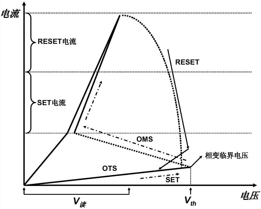
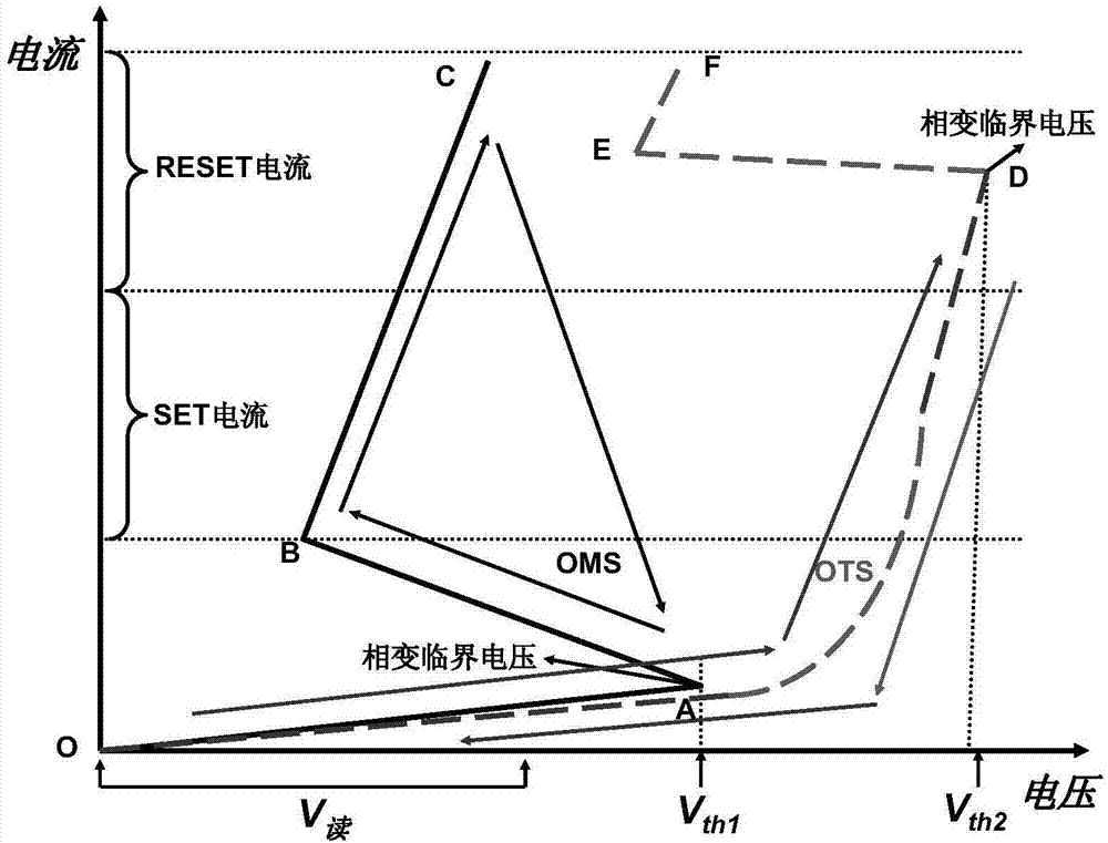
[0037] The present invention also provides a gate driving device, which includes the phase change material as described in the first embodiment. The gate drive device is turned on and off by using the OTS switching characteristics of the phase change material as described in Embodiment 1. At the same time, when the gate drive device is in the on state, the conductive channel formed by arsenic atom doping can provide a large driving force. The current is used to drive the phase change of the phase change memory unit to realize the storage and erasing of information; the gate drive device using the phase change material can realize three-dimensional integration, thereby greatly improving the integration degree and storage density of the memory.

[0038] In summary, the present invention provides a phase change material for a gate drive device, a gate drive device and a preparation method thereof. The general formula of the phase change material for a gate drive device is: Y 1-x ...


PUM


Abstract

The invention provides a phase change material for a gate driving device, the gate driving device and a preparation method thereof. The general formula of the phase change material for the gate driving device is Y1-xAsx, wherein Y is a phase change material which comprises at least one sixth main group element, 0<x<=0.3. According to the phase change material for the gate driving device, through doping arsenic atoms in the phase change material, a conductive material can be formed in the phase change material, thereby increasing phase change critical voltage of the phase change material and current density after switching-on. When the phase change material is used for the gate driving device, switching-on and switching-off are realized through an OTS switching characteristic of the phase change material. Furthermore when the gate driving device is in the on state, the conductive channel which is formed through doping the arsenic atoms can supply large driving current, thereby driving phase change of a phase change memory unit and realizing storage and erasing of information. The gate driving device which uses the phase change material can realize three-dimensional integration, thereby greatly improving integration degree and storage density of the memory.

Description

technical field [0001] The invention belongs to the technical field of microelectronics, and in particular relates to a phase change material used for a gate drive device, a gate drive device and a preparation method thereof. Background technique [0002] Phase-change memory technology is based on the idea that phase-change thin films can be applied to phase-change storage media proposed by Ovshinsky in the late 1960s and early 1970s. It is a memory device with low price and stable performance. Phase-change memory can be made on a silicon wafer substrate, and its key materials are recordable phase-change films, heating electrode materials, heat insulating materials, and lead-out electrode materials. The basic principle of phase change memory is to use electric pulse signal to act on the device unit, so that the phase change material undergoes reversible phase transition between amorphous state and polycrystalline state. By distinguishing the high resistance in the amorphous ...

Claims


Application Information

Patent Timeline
IPC IPC(8): H01L45/00
CPCH10N70/881H10N70/021H10N70/041
Inventor 刘波宋志棠封松林
Owner SHANGHAI INST OF MICROSYSTEM & INFORMATION TECH CHINESE ACAD OF SCI
Why Eureka
Try Eureka