Preparation method of narrow-band-gap-distribution high-purity semi-conductivity single-walled carbon nanotube

A single-walled carbon nanotube, semiconducting technology, applied in the field of controllable preparation of semiconducting single-walled carbon nanotubes, can solve problems such as easy agglomeration, wide diameter distribution, and uncertain nucleation mode

Active Publication Date: 2017-08-25
INST OF METAL RESEARCH - CHINESE ACAD OF SCI
View PDF4 Cites 6 Cited by
  • Summary
  • Abstract
  • Description
  • Claims
  • Application Information

AI Technical Summary

Problems solved by technology

[0005] The purpose of the present invention is to provide a method for preparing narrow bandgap distribution and high-purity semiconducting single-walled carbon nanotubes by partially carbon-coating metal catalysts, which overcomes the problem of uncertain nucleation modes of existing single-walled carbon nanotubes on metal catalysts. The problem of wide diameter distribution of carbon nanotubes, while overcoming the problem of wide diameter distribution caused by the easy agglomeration of existing metallic catalysts at high temperatures, through the size control and structural design of the catalyst, combined with hydrogen in-situ etching, directly grow narrow band gap distribution, high Pure, high-quality semiconducting single-walled carbon nanotubes

Method used


Image

  • Preparation method of narrow-band-gap-distribution high-purity semi-conductivity single-walled carbon nanotube
  • Preparation method of narrow-band-gap-distribution high-purity semi-conductivity single-walled carbon nanotube
  • Preparation method of narrow-band-gap-distribution high-purity semi-conductivity single-walled carbon nanotube

Examples


Embodiment 1

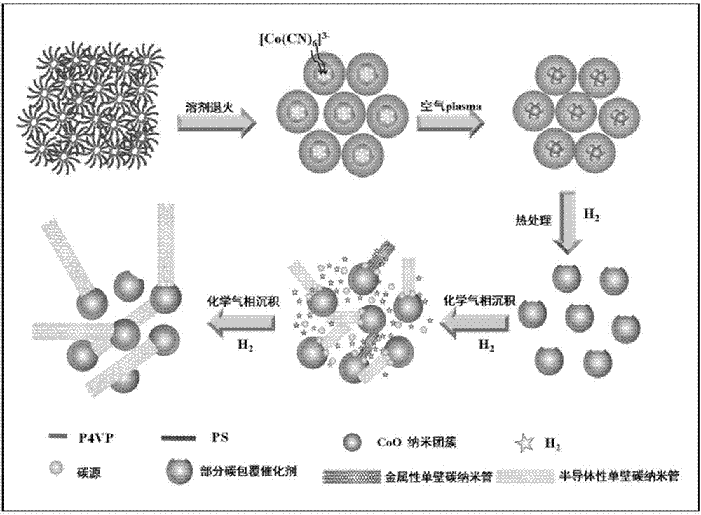
[0045] Example 1. Preparation of partially carbon-coated cobalt nanoparticles and its catalytic growth of narrow bandgap distribution, high-purity semiconducting single-walled carbon nanotubes

[0046] The specific preparation and growth process are as follows: figure 1 shown.

[0047] (1) Preparation of partially carbon-coated Co metal nanoparticles

[0048] The toluene and tetrahydrofuran solution (mass ratio of toluene and tetrahydrofuran 2:1) containing 0.3wt% block copolymer was spin-coated on the surface of the silicon wafer after hydrophilic treatment with 4000rpm, and then placed in toluene and tetrahydrofuran solution (volume ratio 1 :3) Solvent annealing in the vapor of 20 hours, then this silicon chip is placed in 1mM K 3 [Co(CN) 6 ] solution for 3 minutes to adsorb [Co(CN) 6 ] 3- The anions were taken out and washed with deionized water, dried at 60°C for 30 minutes, and finally placed in air plsama (power 20W) for 20 minutes. Place the silicon wafers treated...

Embodiment 2

[0053] Example 2. Preparation of partially carbon-coated iron nanoparticles and its catalytic growth of narrow bandgap distribution, high-purity semiconducting single-walled carbon nanotubes

[0054] (1) Preparation of partially carbon-coated iron metal nanoparticles

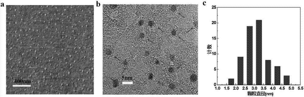
[0055] Catalyst preparation step is consistent with embodiment 1, difference is that catalyst precursor is 1mM K 3 [Fe(CN) 6 ] solution. Atomic force microscopy characterization showed that the nanoparticles were uniformly dispersed on the surface of the silicon substrate. The transmission electron microscope observation shows that the surface of all the nanoparticles is partially covered by the carbon layer, and the particle size is uniform. The diameters of 125 particles randomly counted are distributed in the range of 2.5 to 4.0 nm.

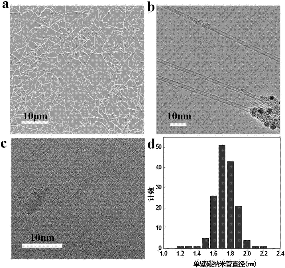
[0056] (2) Growth and characterization of narrow bandgap distribution, high-purity semiconducting single-walled carbon nanotubes

[0057] The growth and characterization of...

Embodiment 3

[0060] Example 3. Preparation of partially carbon-coated iron-tungsten nanoparticles and its catalytic growth of narrow bandgap distribution, high-purity semiconducting single-walled carbon nanotubes

[0061] (1) Preparation of partially carbon-coated iron-tungsten metal nanoparticles

[0062] Catalyst preparation step is consistent with embodiment 1, and difference is that catalyst precursor is 0.5mM K 3 [Fe(CN) 6 ] and 0.5mM (NH 4 ) 10 W 12 o 41 mixed solution. Atomic force microscopy characterization showed that the nanoparticles were uniformly dispersed on the surface of the silicon substrate. The transmission electron microscope observation shows that the surface of all the nanoparticles is partially covered by the carbon layer, and the particle size is uniform. The diameters of 135 particles randomly counted are distributed in the range of 3.0-4.5nm.

[0063] (2) Growth and characterization of narrow bandgap distribution, high-purity semiconducting single-walled ...


PUM

PropertyMeasurementUnit
sizeaaaaaaaaaa
particle sizeaaaaaaaaaa
particle diameteraaaaaaaaaa

Abstract

The invention relates to the field of controlled preparation of semi-conductivity single-walled carbon nanotubes, in particular to a method for preparing a narrow-band-gap-distribution high-purity semi-conductivity single-walled carbon nanotube through a partial-carbon-coated metal catalyst. By means of a segmented copolymer self-assembly method, a uniform-size copolymer thin film coated metal anion nanometer cluster is prepared; single-dispersion partial-carbon-coated metal catalyst nanoparticles are obtained by controlling the annealing, oxidizing and reducing conditions of solvents; nitrogen serves as in-situ etching gas, and the narrow-band-gap-distribution high-purity semi-conductivity single-walled carbon nanotube directly grows. The content of the semi-conductivity single-walled carbon nanotube is larger than 98%, and the band gap difference is 0.05 eV at least and can be adjusted. The direct controllable growth of the narrow-band-gap-distribution high-purity semi-conductivity single-walled carbon nanotube is achieved, the bottleneck of control and preparation of the narrow-band-gap-distribution high-purity semi-conductivity single-walled carbon nanotube at the present stage is broken through, and it is proved that the nanotube is an ideal tunnel material for establishing a thin film field effect transistor.

Description

technical field [0001] The invention relates to the field of controllable preparation of semiconducting single-walled carbon nanotubes, specifically a method for preparing semiconducting single-walled carbon nanotubes with narrow bandgap distribution and high purity by partially carbon-coated metal catalysts. Assembly process and post-treatment conditions to prepare monodisperse, narrow particle size distribution, partially carbon-coated metal catalyst nanoparticles; then use hydrogen as a carrier gas and etching gas to remove highly active metallic single-walled carbon nanotubes in situ , to directly realize the controlled growth of semiconducting single-walled carbon nanotubes with narrow bandgap distribution and tunable bandgap. Background technique [0002] Single-walled carbon nanotubes can be regarded as one-dimensional hollow tubular structures rolled from single-layer graphene, which have metallic or semiconducting properties related to diameter and helix angle. Sem...

Claims


Application Information

Patent Timeline
Patent Type & Authority Applications(China)
IPC IPC(8): C01B32/162C01B32/159B01J23/75B01J23/745B01J23/888B01J23/89
CPCB01J23/745B01J23/75B01J23/888B01J23/8993B01J35/023C01P2002/82C01P2004/04
Inventor 刘畅张峰侯鹏翔成会明
Owner INST OF METAL RESEARCH - CHINESE ACAD OF SCI
Why Eureka
Try Eureka