

Method for preparing fixed-point replaced amorphous nanowire array with Si
A nanowire array and amorphous technology, which is applied in the field of template-free preparation of Si fixed-point replacement of amorphous nanowire arrays, can solve the problems that are not conducive to carrier transfer to the surface, reduce photocatalytic efficiency, and harsh preparation conditions, etc. The effect of novel and uniform appearance, high light utilization efficiency, and simple preparation process
- Summary
- Abstract
- Description
- Claims
- Application Information
AI Technical Summary
Problems solved by technology
Method used
Image

Examples
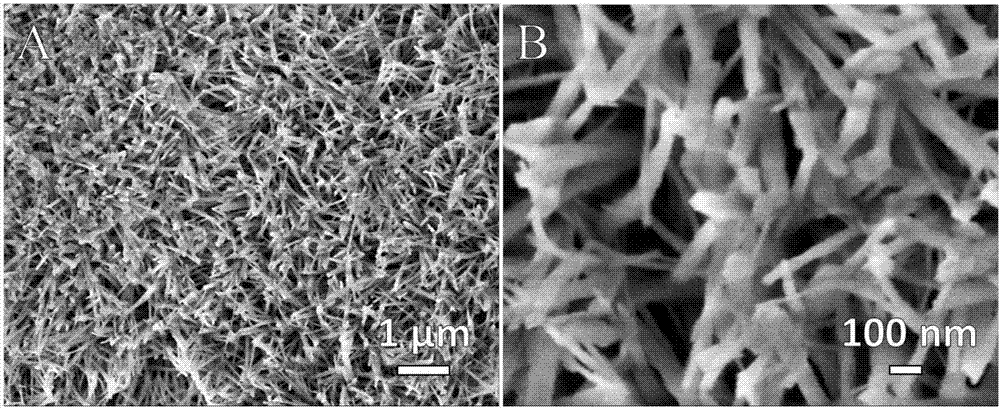
Embodiment 1
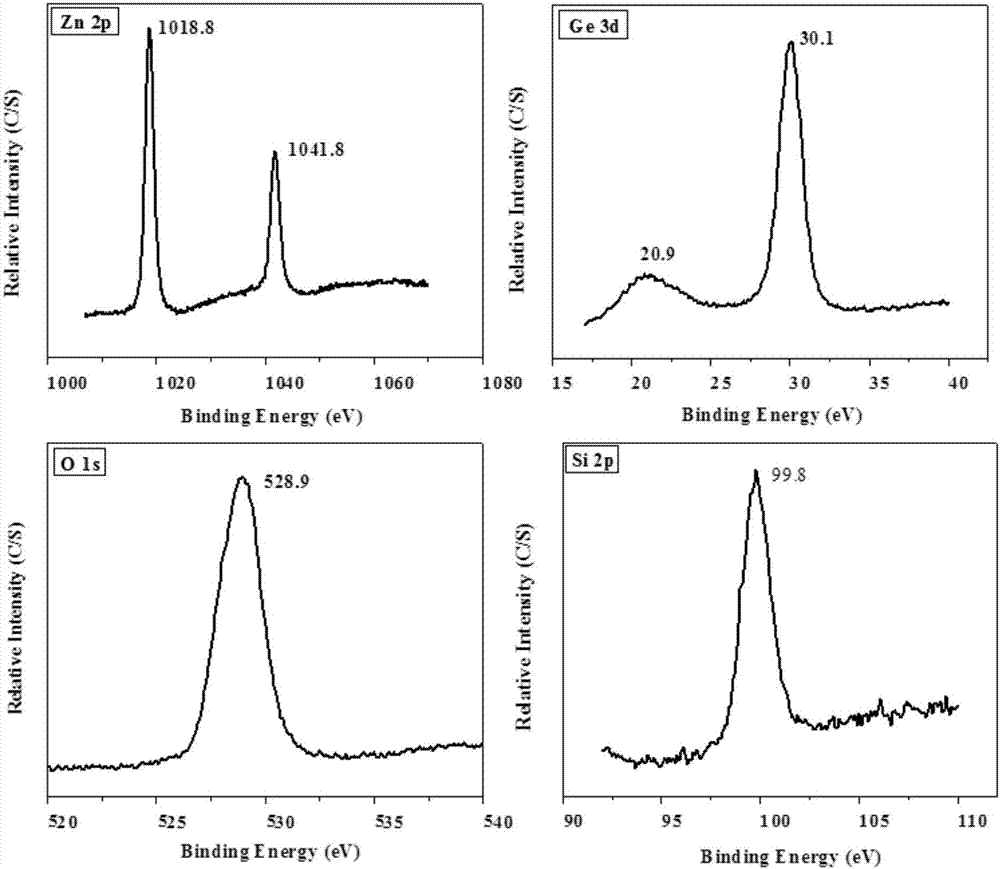
[0029] 0.55g of zinc acetate and 0.13g of germanium oxide were weighed and added to a mixed solvent of 10ml of water and 20ml of ethylenediamine. Stir magnetically at room temperature for one hour at a stirring rate of 600 r / min. Transfer the mixed solution to a 50ml reaction kettle, and put into a single crystal Si chip (1.5*3cm 2 ), hydrothermal reaction at 150°C for 10h. After cooling to room temperature, the product was washed alternately with ethanol and deionized water. The samples prepared as figure 1 As shown in A, it is a nanowire array structure with uniform shape and stable structure. It can be observed from 1B that the diameter of the nanowire array is about 40-60 nm.
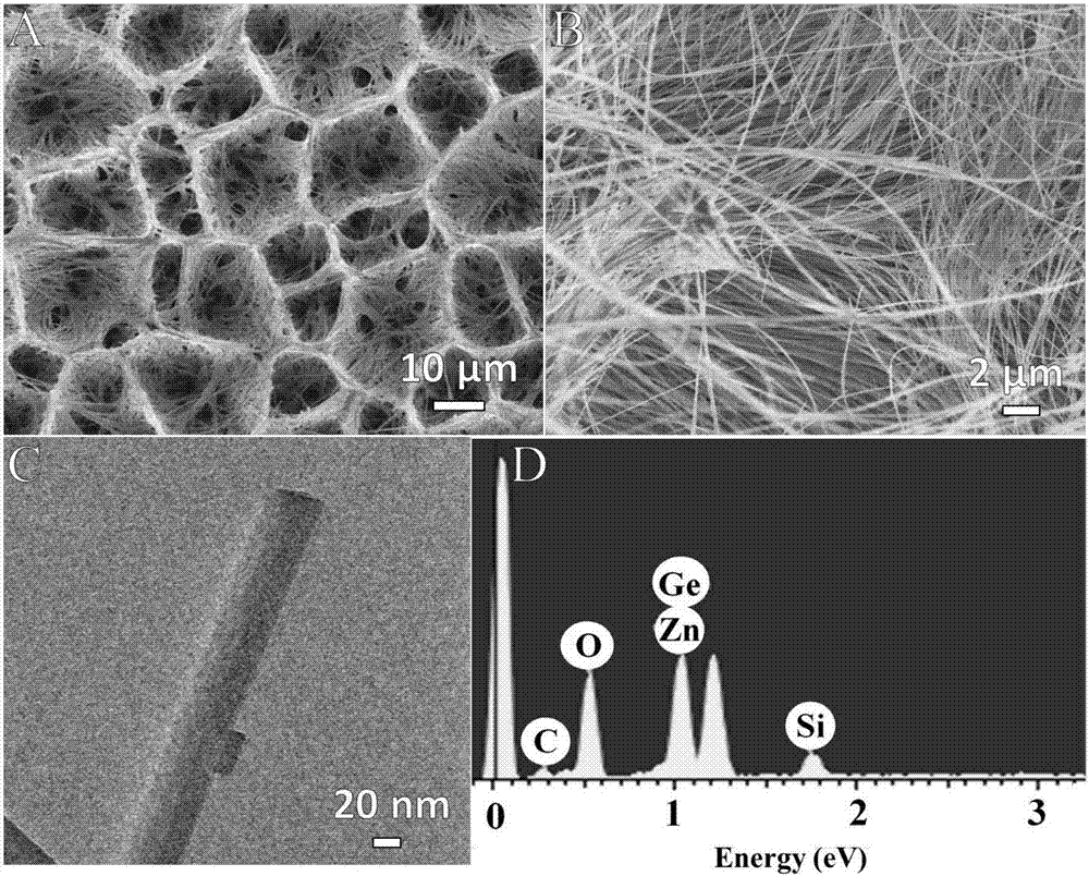
Embodiment 2
[0031] 0.55g of zinc acetate and 0.13g of germanium oxide were weighed and added to a mixed solvent of 10ml of water and 20ml of ethylenediamine. Stir magnetically at room temperature for one hour at a stirring rate of 800 r / min. Transfer the mixed solution to a 50ml reaction kettle, and put into a single crystal Si chip (1.5*3cm 2 ), 180°C hydrothermal reaction for 15h. After cooling to room temperature, the product was washed alternately with ethanol and deionized water. The samples prepared as figure 2 As shown in A, it is a honeycomb nanowire array structure. The product has a unique shape and is evenly distributed.
Embodiment 3
[0033] 0.55g of zinc acetate and 0.13g of germanium oxide were weighed and added to a mixed solvent of 10ml of water and 20ml of ethylenediamine. Stir magnetically at room temperature for one hour at a stirring rate of 1000 r / min. Transfer the mixed solution to a 50ml reaction kettle, and put into a single crystal Si chip (1.5*3cm 2 ), 180 degree hydrothermal reaction for 20h. After cooling to room temperature, the product was washed alternately with ethanol and deionized water. The samples prepared as figure 2 As shown in B, it is an ultra-long nanowire array with a length of about tens of microns.
PUM
| Property | Measurement | Unit |
|---|---|---|
| diameter | aaaaa | aaaaa |
| diameter | aaaaa | aaaaa |
Abstract
Description
Claims
Application Information