Thin film bulk acoustic resonator and its processing method

A thin-film bulk acoustic wave and resonator technology, applied in impedance networks, electrical components, etc., can solve the problems affecting the performance of thin-film bulk acoustic wave resonators, affecting the growth of high-quality piezoelectric layers, etc., to avoid incomplete release and adhesion problems. , get high effect

Active Publication Date: 2020-08-11
HANGZHOU SAPPLAND MICROELECTRONICS TECH CO LTD
View PDF2 Cites 0 Cited by
  • Summary
  • Abstract
  • Description
  • Claims
  • Application Information

AI Technical Summary

Problems solved by technology

Since the deposition quality of the piezoelectric layer (such as crystal orientation, surface flatness, etc.) largely depends on the quality of the bottom electrode, especially defects such as residues and burrs on the edge of the bottom electrode caused by etching will seriously affect the quality of the piezoelectric layer. layer growth, thereby affecting the performance of the final thin-film bulk acoustic resonator

Method used


Image

  • Thin film bulk acoustic resonator and its processing method
  • Thin film bulk acoustic resonator and its processing method
  • Thin film bulk acoustic resonator and its processing method

Examples


Embodiment 1

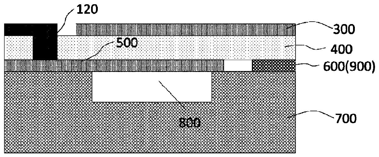
[0030] figure 1 It is a cross-sectional structure diagram of a thin film bulk acoustic resonator according to an embodiment of the present invention, the thin film bulk acoustic resonator includes a substrate 700, the substrate 700 is, for example, a silicon wafer; the substrate 700 includes an air gap 800; a bonding layer 600 (900), bonding layer is for example gold etc.; Including piezoelectric sandwich structure above air gap 800, wherein 500 is the first electrode of piezoelectric sandwich structure, and material is molybdenum etc.; 400 is the piezoelectric layer of piezoelectric sandwich structure , the material is a piezoelectric single crystal, such as piezoelectric quartz, lithium tantalate, lithium niobate or lithium tetraborate, etc.; 300 is the second electrode of the piezoelectric sandwich structure, and the material is molybdenum, etc.; the interconnection metal 120 is the piezoelectric sandwich The first electrode of the structure is led out to the surface of 400...

Embodiment 2

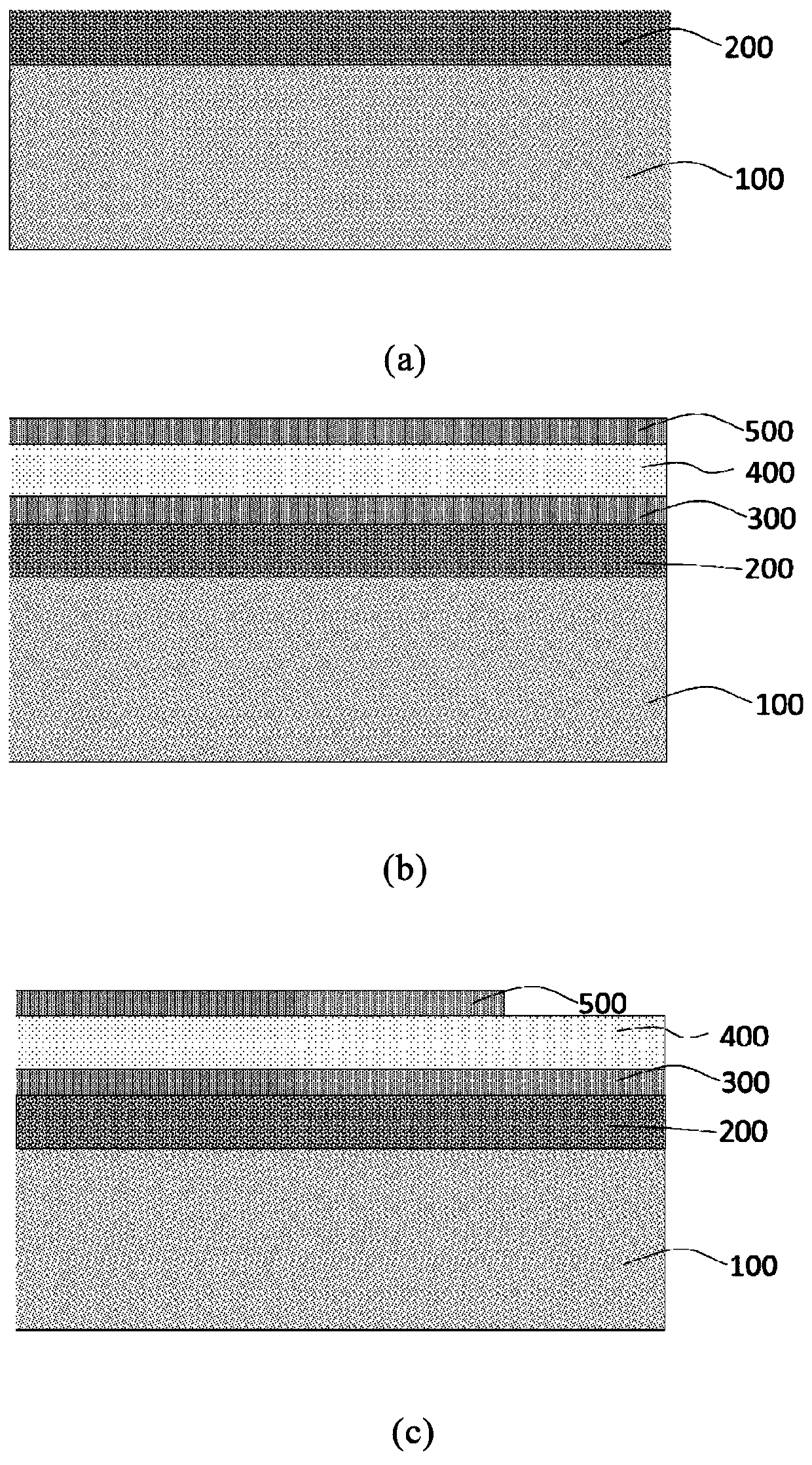
[0032] figure 2 It is a flow chart of the preparation process of a thin film bulk acoustic resonator according to an embodiment of the present invention, and the preparation process includes:

[0033] (a) Prepare a silicon wafer 100 polished on one or both sides, with the polished side up, and perform standard cleaning.

[0034] (b) Depositing a layer of thin film material 200 for subsequent peeling. The material can be silicon dioxide, silicon nitride, phosphosilicate glass and other materials that are easy to peel off from the silicon substrate.

[0035] (c) Depositing the second electrode 300 , the piezoelectric material 400 and the first electrode 500 sequentially on the thin film material 200 . Wherein, the first electrode 500 and the second electrode 300 include molybdenum electrodes, and the piezoelectric material 400 includes one or a combination of aluminum nitride (AlN), zinc oxide (ZnO), lithium niobate (LiNbO3), lithium tantalate (LiTaO3) .

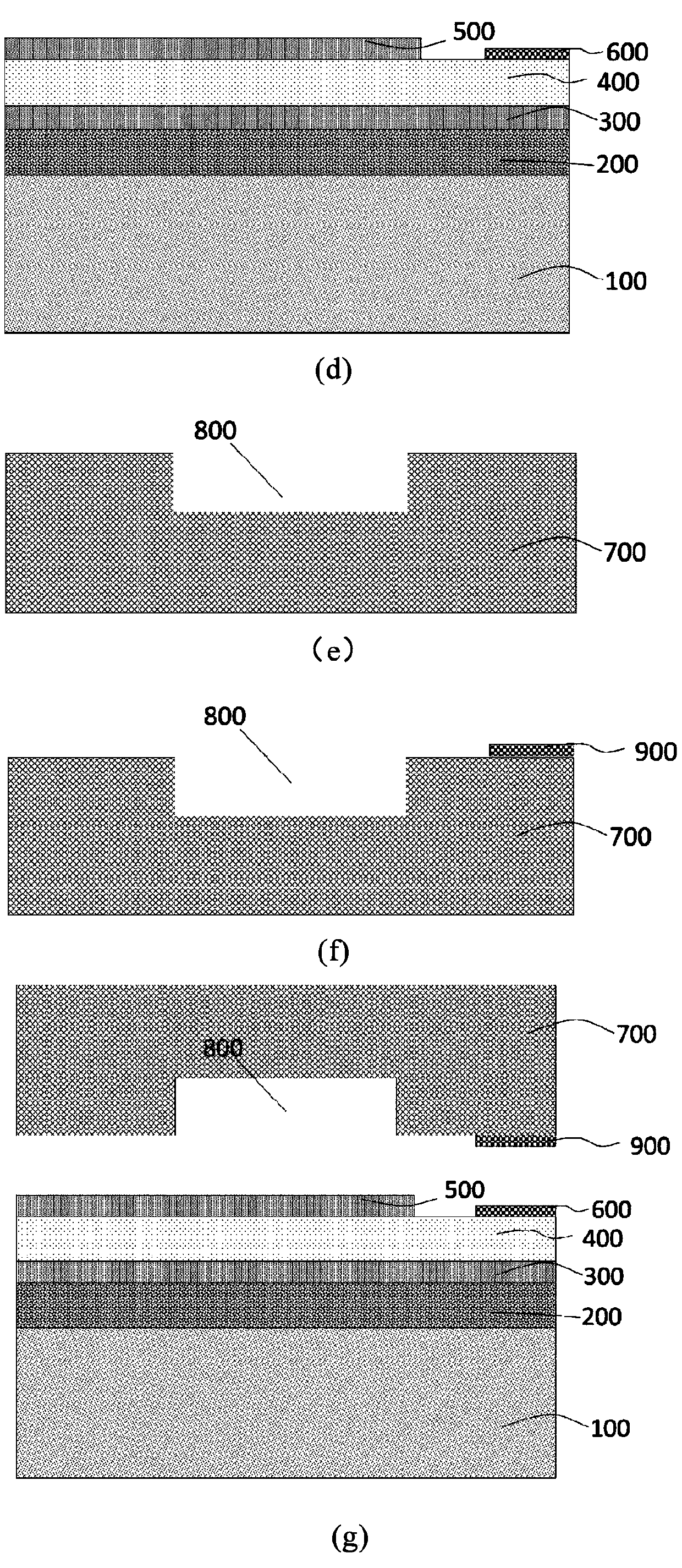
[0036] (d) pattern...


PUM


Abstract

The invention discloses a film bulk acoustic resonator, which is realized through a bonding way, and a processing method thereof. The method comprises the following steps of depositing a top electrode, a piezoelectric material and a bottom electrode in sequence to form a piezoelectric film stacking structure, etching the bottom electrode and bonding the bottom electrode with a substrate with a cavity, and lastly, etching top electrode metal to form a needed electrode shape. According to the preparation method provided by the invention, a piezoelectric sandwich structure is deposited and is integrally etched, so that the defect or the damage caused by depositing a piezoelectric material layer is effectively avoided, and furthermore, a pre-etched cavity bonding process is adopted, so that the problems of incomplete sacrificial layer release and adhesion which are caused by the conventional processing method or device stress caused by back etching can be effectively avoided.

Description

technical field [0001] The invention relates to a thin-film bulk acoustic wave resonator, in particular to a thin-film bulk acoustic wave resonator realized by bonding technology and a processing method thereof. Background technique [0002] With the development of wireless communication applications, people have higher and higher requirements for data transmission speed. In the field of mobile communication, the first generation is analog technology, the second generation realizes digital voice communication, the third generation (3G) is characterized by multimedia communication, and the fourth generation (4G) increases the communication rate to 1Gbps and reduces the delay By 10ms, the fifth generation (5G) is a new generation of mobile communication technology after 4G. Although the technical specifications and standards of 5G have not yet been fully clarified, compared with 3G and 4G, its network transmission rate and network capacity will be greatly improved. If the mai...

Claims


Application Information

Patent Timeline
Patent Type & Authority Patents(China)
IPC IPC(8): H03H3/02H03H9/13H03H9/17
CPCH03H3/02H03H9/13H03H9/173H03H9/174H03H2003/023
Inventor 张树民王国浩陈海龙
Owner HANGZHOU SAPPLAND MICROELECTRONICS TECH CO LTD
Why Eureka
Try Eureka