Ferroelectric field-effect transistor and preparation method thereof
An electric field effect and transistor technology, which is applied in the field of ferroelectric field effect transistors and their preparation, can solve the problem that the performance of FeFET does not meet commercialization requirements, increases the cross-contamination between ferroelectric thin films and silicon integrated circuits, and the incompatibility of field effect transistor preparation processes, etc. problems, to achieve the effect of not easy leakage and breakdown, excellent ferroelectricity, and good compatibility
- Summary
- Abstract
- Description
- Claims
- Application Information
AI Technical Summary
Problems solved by technology
Method used
Image

Examples
Embodiment 1
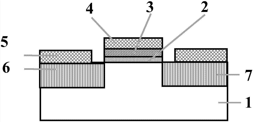
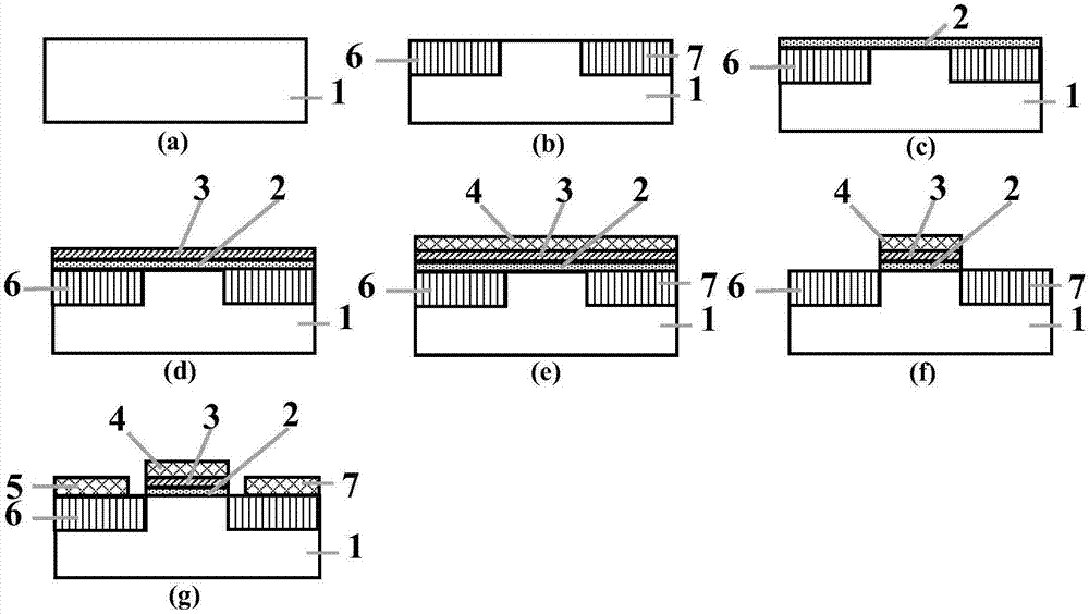
[0050] An embodiment of the ferroelectric field effect transistor of the present invention, a cross-sectional structure diagram of the ferroelectric field effect transistor described in this embodiment is shown in the attached figure 1 shown, including:
[0051] substrate1;
[0052] a source region 6 formed on the substrate 1;
[0053] a drain region 7 formed on the substrate 1 and separated from the source region 6;
[0054] an insulating layer 2 formed on the substrate 1 and between the source region 6 and the drain region 7;
[0055] A ferroelectric thin film layer 3 formed on the insulating layer 2;
[0056] A gate electrode 4 formed on the ferroelectric thin film layer 3;
[0057] a source electrode 5 formed on the source region 6;
[0058] as well as
[0059] A drain electrode 8 is formed on the drain region 7 .
[0060] Wherein, the ferroelectric thin film layer 3 is composed of a hafnium oxide-based material, and the hafnium oxide-based material is Zr-doped HfO ...
Embodiment 2
[0079] An embodiment of the ferroelectric field effect transistor of the present invention, a cross-sectional structure diagram of the ferroelectric field effect transistor described in this embodiment is shown in the attached figure 1 shown, including:
[0080] substrate1;
[0081] a source region 6 formed on the substrate 1;
[0082] a drain region 7 formed on the substrate 1 and separated from the source region 6;
[0083] an insulating layer 2 formed on the substrate 1 and between the source region 6 and the drain region 7;
[0084] A ferroelectric thin film layer 3 formed on the insulating layer 2;
[0085] A gate electrode 4 formed on the ferroelectric thin film layer 3;
[0086] a source electrode 5 formed on the source region 6;
[0087] as well as
[0088] A drain electrode 8 is formed on the drain region 7 .
[0089] Wherein, the ferroelectric thin film layer 3 is composed of a hafnium oxide-based material, and the hafnium oxide-based material is Si-doped HfO ...
Embodiment 3
[0108] An embodiment of the ferroelectric field effect transistor of the present invention, a cross-sectional structure diagram of the ferroelectric field effect transistor described in this embodiment is shown in the attached figure 1 shown, including:
[0109] substrate1;
[0110] a source region 6 formed on the substrate 1;
[0111] a drain region 7 formed on the substrate 1 and separated from the source region 6;
[0112] an insulating layer 2 formed on the substrate 1 and between the source region 6 and the drain region 7;
[0113] A ferroelectric thin film layer 3 formed on the insulating layer 2;
[0114] A gate electrode 4 formed on the ferroelectric thin film layer 3;
[0115] a source electrode 5 formed on the source region 6;
[0116] as well as
[0117] A drain electrode 8 is formed on the drain region 7 .
[0118] Wherein, the ferroelectric thin film layer 3 is composed of a hafnium oxide-based material, and the hafnium oxide-based material is Al-doped HfO 2...
PUM
| Property | Measurement | Unit |
|---|---|---|
| Thickness | aaaaa | aaaaa |
| Thickness | aaaaa | aaaaa |
| Thickness | aaaaa | aaaaa |
Abstract
Description
Claims
Application Information
 - R&D
- Intellectual Property
- Life Sciences
- Materials
- Tech Scout
- Unparalleled Data Quality
- Higher Quality Content
- 60% Fewer Hallucinations
Browse by: Latest US Patents, China's latest patents, Technical Efficacy Thesaurus, Application Domain, Technology Topic, Popular Technical Reports.
© 2025 PatSnap. All rights reserved.Legal|Privacy policy|Modern Slavery Act Transparency Statement|Sitemap|About US| Contact US: help@patsnap.com