A silicon carbide trenchmos device and manufacturing method thereof

A silicon carbide and device technology, which is applied in semiconductor/solid-state device manufacturing, semiconductor devices, electrical components, etc., can solve problems such as low work efficiency, high power loss, and high production cost

Active Publication Date: 2019-11-01
HANGZHOU SILICON-MAGIC SEMICON TECH CO LTD
View PDF2 Cites 0 Cited by
  • Summary
  • Abstract
  • Description
  • Claims
  • Application Information

AI Technical Summary

Problems solved by technology

The present invention adds a convex polysilicon region inside the epitaxial layer, and sets two independent trench gates in the groove of the convex polysilicon region, thereby making the polysilicon layer and the epitaxial layer form a Si / SiC heterojunction; using the present invention Silicon carbide Trench MOS devices in the above circuits can overcome the problems of high power loss, low work efficiency, and high production costs in the prior art

Method used


Image

  • A silicon carbide trenchmos device and manufacturing method thereof
  • A silicon carbide trenchmos device and manufacturing method thereof
  • A silicon carbide trenchmos device and manufacturing method thereof

Examples


Embodiment 1

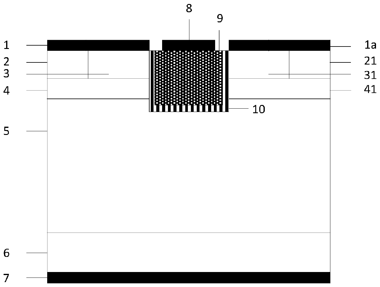
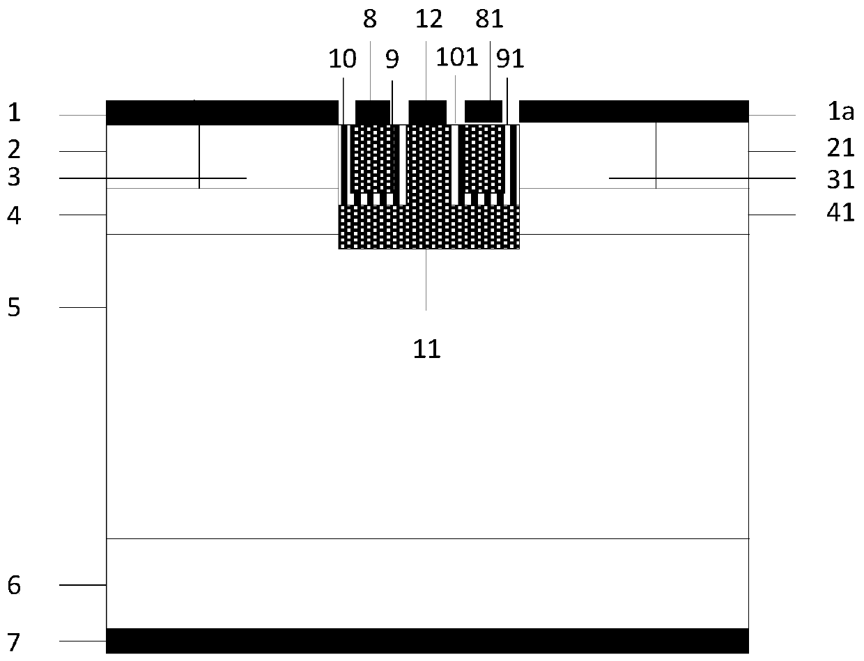
[0099] A silicon carbide Trench MOS device, its cell structure is as follows figure 2 Shown includes: metal drain electrodes 7, N + Substrate 6 and N - epitaxial layer 5; the N - One end of the upper layer of the epitaxial layer 5 has a first Pbase region 4, the N - The other end of the upper layer of the epitaxial layer 5 has a second Pbase region 41; the first Pbase region 4 has mutually independent first N + source region 3 and the first P + Contact region 2; the second Pbase region 41 has second N independent of each other + source region 31 and the second P + Contact area 21; the first P + contact zone 2 and the first N + The upper surface of the source region 3 has a first metal source electrode 1; the second P + contact region 21 and the second N + The upper surface of the source region 31 has a second metal source electrode 1a; it is characterized in that: the N under the middle position of the two Pbase regions 4, 41 - There is a convex P-type polysilicon re...

Embodiment 2

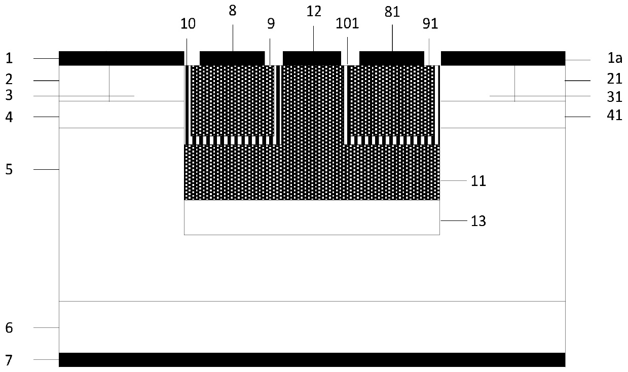
[0102] In this implementation, on the basis of Embodiment 1, there is also a P+ silicon carbide region 13 in contact with it below the P-type polysilicon region 11; the width of the P+ silicon carbide region 13 is the same as that of the P-type polysilicon region 11 .

[0103] The P+ silicon carbide region 13 added in this embodiment can shield the P+ polysilicon region 11 and the MOS trench gate from the electric field, thereby improving the withstand voltage of the device, and has a certain effect on suppressing the reverse leakage current.

Embodiment 3

[0105] In this implementation, on the basis of Embodiment 1, there is also a P + SiC region 13; the P + The width of the silicon carbide region 13 is greater than the width of the P-type polysilicon region 11, the P + The width of the silicon carbide region 13 ranges from 1.0 to 2.6 μm.

[0106] In this example, P + The lateral dimension (i.e. width) of the silicon carbide region 13 is enlarged, and compared with the embodiment 2, it has a stronger electric field shielding effect on the P+ polysilicon region 11 and the MOS trench gate, further improves the withstand voltage of the device, and further suppresses the reverse leakage current.


PUM

PropertyMeasurementUnit
thicknessaaaaaaaaaa
thicknessaaaaaaaaaa
thicknessaaaaaaaaaa

Abstract

The invention discloses a silicon carbide Trench MOS device and a manufacturing method thereof, belonging to the technical field of power semiconductors. In the present invention, a convex polysilicon region is added inside the epitaxial layer, and two independent trench gates are arranged in the groove of the convex polysilicon region, so that the polysilicon layer and the epitaxial layer form a Si / SiC heterojunction. Compared with the parasitic silicon carbide diode directly using silicon carbide Trench MOS, the present invention significantly reduces the junction voltage drop when the device diode is applied, and the larger heterojunction area improves the conduction characteristics of the device; the present invention is based on convex polysilicon The charge shielding effect of the region reduces the ratio of its gate-drain capacitance and gate-drain to gate-source capacitance, significantly improving the performance and reliability of the device; the device of the present invention is unipolar conduction, so it also has better The reverse recovery performance also has the advantages of low reverse leakage, high breakdown voltage and good temperature stability of traditional Trench MOS devices, so the invention has broad prospects in inverter circuits, chopper circuits and other circuits.

Description

technical field [0001] The invention belongs to the technical field of power semiconductors, and in particular relates to a silicon carbide Trench MOS device and a manufacturing method thereof. Background technique [0002] Today, when the global greenhouse effect is becoming more serious and the call for energy conservation and emission reduction is increasing, the problem of electric energy conversion in household appliances, electric vehicles, industrial production, and locomotive traction is particularly important. In order to improve the efficiency of electric energy use, the field of power electronics It is imminent for scientific researchers to optimize and improve the power system. [0003] Power devices are at the heart of modern power systems. Since the performance of traditional silicon-based power devices is already very close to the limit of silicon materials, it is difficult to greatly improve their performance. In order to meet the application requirements o...

Claims


Application Information

Patent Timeline
Patent Type & Authority Patents(China)
IPC IPC(8): H01L29/78H01L29/423H01L29/06H01L29/16H01L21/336
CPCH01L29/0615H01L29/0684H01L29/1608H01L29/4236H01L29/66477H01L29/7831
Inventor 张金平邹华刘竞秀李泽宏任敏张波
Owner HANGZHOU SILICON-MAGIC SEMICON TECH CO LTD
Why Eureka
Try Eureka