Top-emitting-type OLED panel manufacturing method and structure thereof

A manufacturing method and top-emission technology, applied in the field of OLED display, can solve problems such as high risk of defective problems, complicated etching process, and multi-mask number, etc., achieve low risk of defective problems, save the number of photomasks, and simplify the manufacturing process Effect

Inactive Publication Date: 2017-10-24
SHENZHEN CHINA STAR OPTOELECTRONICS SEMICON DISPLAY TECH CO LTD
View PDF7 Cites 28 Cited by
  • Summary
  • Abstract
  • Description
  • Claims
  • Application Information

AI Technical Summary

Problems solved by technology

The composite conductive film used only as an anode usually adopts a sandwich structure of indium tin oxide / silver / indium tin oxide (ITO / Ag / ITO) to reflect light by using Ag. The etching process of this type of anode is relatively complicated and occurs Greater risk of adverse issues
[0005] At present, the common technical route for OLED panel production is to deposit the red, green, blue (Red, Green, Blue, RGB) OLED light-emitting layer of the three primary colors of the OLED through the vacuum thermal evaporation process. The advantages are simple and mature process and easy operation. But in the preparation High-resolution displays require high-precision masks and precise alignment, resulting in lower production capacity and higher costs; moreover, the existing OLED panels have a large number of structural layers, such as light-shielding layers, flat layers, and pixel definition layers etc. In addition, the anode is specially made by a separate relatively complex yellow light process. The existing OLED panel production method requires a large number of masks, a relatively complicated process, and a high production cost.

Method used


Image

  • Top-emitting-type OLED panel manufacturing method and structure thereof
  • Top-emitting-type OLED panel manufacturing method and structure thereof
  • Top-emitting-type OLED panel manufacturing method and structure thereof

Examples


Embodiment Construction

[0060] In order to further illustrate the technical means adopted by the present invention and its effects, the following describes in detail in conjunction with preferred embodiments of the present invention and accompanying drawings.

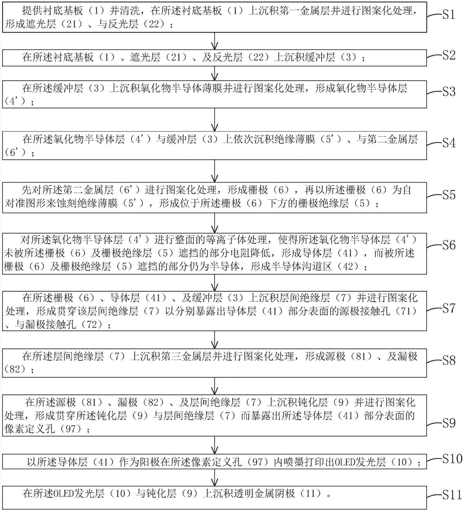
[0061] see figure 1 , the present invention firstly provides a method for manufacturing a top-emitting OLED panel, comprising the following steps:

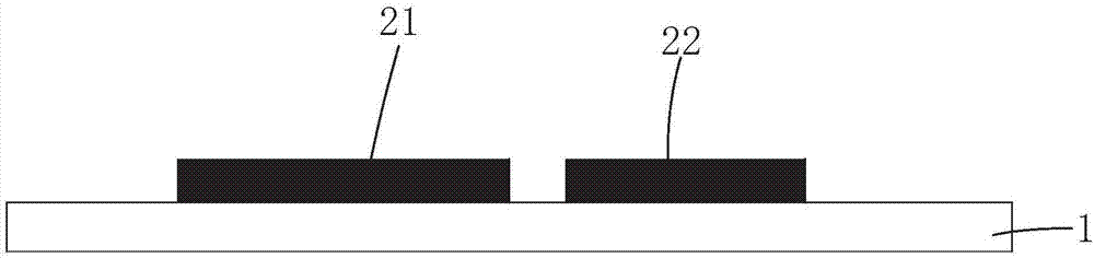
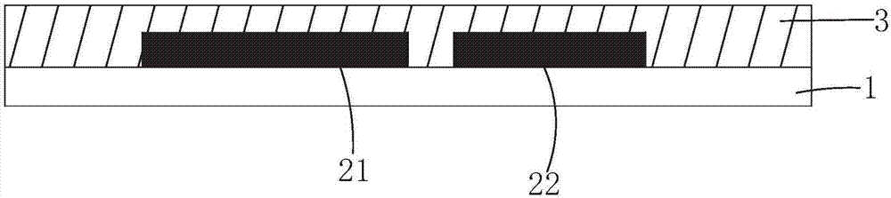
[0062] Step S1, such as figure 2 As shown, the base substrate 1 is provided and cleaned, the first metal layer is deposited on the base substrate 1 and patterned through yellow light and etching processes, and a light shielding layer 21 is formed in the area corresponding to the thin film transistor to be fabricated. A reflective layer 22 is formed in a region corresponding to the OLED to be fabricated.

[0063] Specifically, the base substrate 1 is preferably a glass substrate; the material of the first metal layer is one or more alloys of molybdenum (Mo), aluminum (Al), copper (Cu), and titan...


PUM


Abstract

The present invention provides a top-emitting-type OLED panel manufacturing method and the structure thereof. In the top-emitting-type OLED panel manufacturing method, through the patterned treatment of a first metal layer, a light blocking layer and a light reflecting layer are fabricated, which simplifies the manufacturing technology for an anode and reduces the risk for bad problems. After a gate electrode and a gate electrode insulation layer are fabricated on an oxide semiconductor layer, plasma treatment is performed on the entire surface of the oxide semiconductor layer so that the part of the oxide semiconductor layer not covered by the gate electrode and the gate electrode insulation layer is reduced in resistance and forms a conductor layer, while the part blocked by the gate electrode and the gate electrode insulation layer is still a semiconductor and forms a semiconductor channel region. The conductor layer is used as the anode of a white light OLED, which can eliminate yellow light for fabricating the anode independently and an etching process. In addition, the fabrication of a traditional flattening layer and a pixel defining layer can both be eliminated, therefore, reducing the number of procedures for yellow light fabricating, reducing the number of light covers and cutting the fabricating cost. The use of an ink-jet printing OLED light-emitting layer further keeps the manufacturing cost down.

Description

technical field [0001] The invention relates to the field of OLED display technology, in particular to a method for manufacturing a top-emitting OLED panel and its structure. Background technique [0002] In the field of display technology, flat panel display devices such as Liquid Crystal Display (LCD) and Organic Light Emitting Diode (OLED) have gradually replaced Cathode Ray Tube (CRT) displays. [0003] Among them, OLED panels have many advantages such as self-illumination, low driving voltage, high luminous efficiency, short response time, high definition and contrast, nearly 180° viewing angle, wide operating temperature range, flexible display and large-area full-color display, etc. It is recognized by the industry as the most promising display device. [0004] Existing OLED panels usually include: a substrate, a composite conductive film placed on the substrate only for the anode, a hole injection layer (HIL) placed on the ITO anode, and a hole transport layer place...

Claims


Application Information

Patent Timeline
Patent Type & Authority Applications(China)
IPC IPC(8): H01L27/12H01L27/32H01L29/786H01L21/77
CPCH01L27/1259H01L29/7869H10K59/126
Inventor 刘兆松任章淳
Owner SHENZHEN CHINA STAR OPTOELECTRONICS SEMICON DISPLAY TECH CO LTD
Why Eureka
Try Eureka