Method for preparing ultra-flat copper monocrystalline film

A single crystal thin film and single crystal technology, applied in the direction of single crystal growth, single crystal growth, chemical instruments and methods, etc., can solve problems such as difficulty in preparing large-sized thin films, limiting the application of copper thin films, and damage to copper single crystals, etc. High repeatability, smooth surface, diameter controllable effect

Active Publication Date: 2017-11-17
PEKING UNIV
View PDF3 Cites 24 Cited by
  • Summary
  • Abstract
  • Description
  • Claims
  • Application Information

AI Technical Summary

Problems solved by technology

The length of single crystal castings produced by these methods is limited by the size of the device and crucible, and only rods with limited diameters can be grown, but it is difficult to prepare large-sized films, which severely limits the application of copper films.
In addition, the rods prepared by these methods require additional cutting in some thin film fields, and the cutting may cause certain damage to the copper single crystal
Moreover, these methods are expensive, so they have not been able to achieve a wide range of applications

Method used


Image

  • Method for preparing ultra-flat copper monocrystalline film
  • Method for preparing ultra-flat copper monocrystalline film
  • Method for preparing ultra-flat copper monocrystalline film

Examples


Embodiment 1

[0038] Embodiment 1, preparation of 4 inch copper single crystal by magnetron sputtering

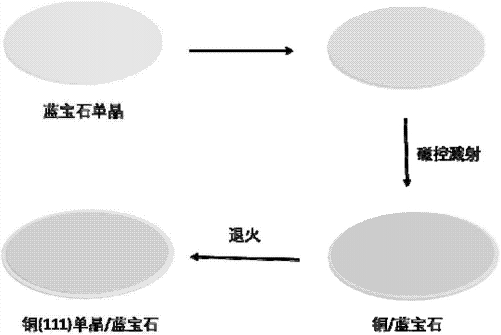
[0039] The overall process is as figure 1 shown.

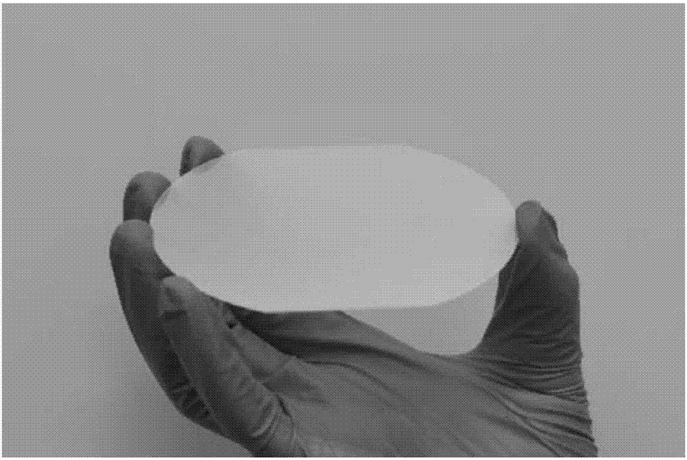
[0040] Step (1): Use a sapphire single crystal purchased from Jiangyin Ruibo Electronic New Material Co., Ltd.; the sapphire single crystal is c-plane (0001); the thickness of the sapphire single crystal is not limited, usually 0.65mm, and the size is 4 inches. its photo as figure 2 shown.

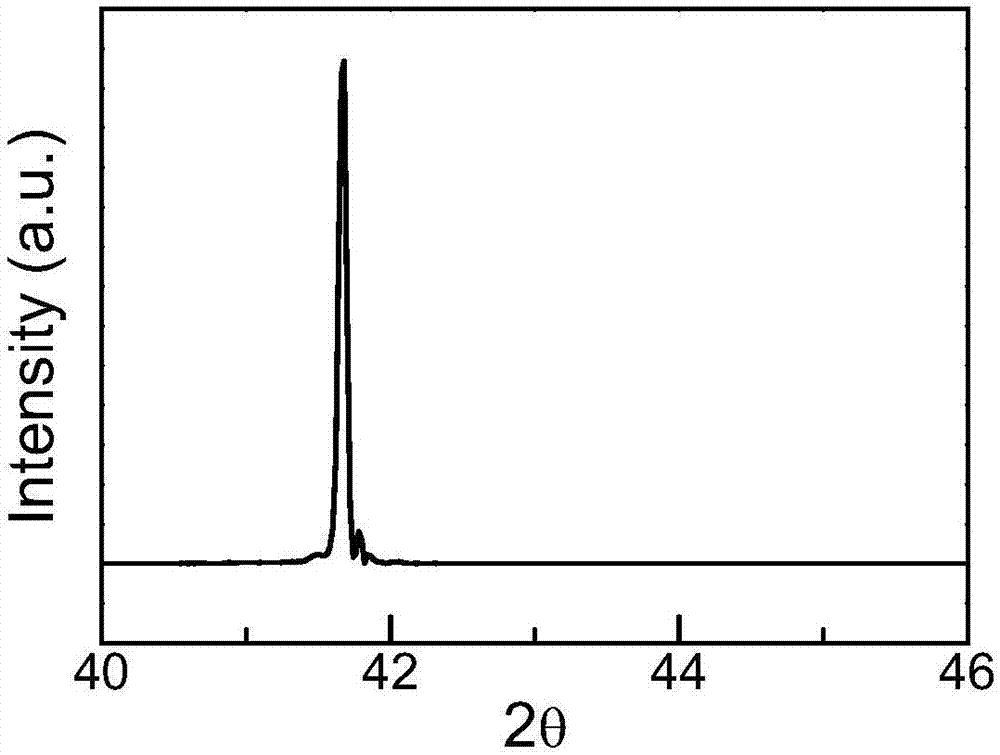
[0041] Step (2): Cleaning to improve the surface state of the sapphire and remove defects, fractures or impurities generated during the cutting process. The cleaning conditions are: phosphoric acid: sulfuric acid = 3.1 (v / v), temperature: 300°C, cleaning time: 1h ; then rinse several times in deionized water, and finally blow dry with a nitrogen gun. The X-ray diffraction pattern of the cleaned sapphire is as follows image 3 As shown, it can be seen that only Al 2 o 3 (0006) peak, indicating that the sapphire used is a single crystal.

[00...

Embodiment 2

[0045] Embodiment 2, preparation of twinned copper single crystal by magnetron sputtering

[0046] 1) step is with embodiment 1 step 1);

[0047] 2) step is the same as embodiment 1 step 2);

[0048] 3) Step: Do not anneal the sapphire single crystal

[0049] 4) step is the same as embodiment 1 step 4);

[0050] 5) step is the same as embodiment 1 step 5); adopt high-resolution X-ray diffraction characterization to the copper after stepping back, its in-plane scanning is as follows Figure 10 As shown in , it can be seen that there are 6 peaks in the plane of copper, which indicates that copper is a single crystal with twins. Electron microscopy was used to characterize the annealed copper, as shown in Figure 11 As shown, it can be seen that the copper surface becomes very flat after annealing, but there are twin grain boundaries. The annealed copper was characterized by atomic force microscopy, as shown in Figure 12 As shown, it can be seen that the copper surface bec...


PUM

PropertyMeasurementUnit
thicknessaaaaaaaaaa

Abstract

The invention discloses a method for preparing an ultra-flat copper monocrystalline film. The method for preparing the copper monocrystalline film, provided by the invention, comprises the following steps: taking a sapphire monocrystal as a growth substrate, carrying out copper target magnetron sputtering, and carrying out annealing, thereby obtaining the copper monocrystalline film. According to the method, sapphire is adopted as an epitaxial substrate of copper, a magnetron sputtering method is adopted, a copper film with consistent orientation is deposited on the surface of a c-face sapphire substrate, and copper with consistent orientation is aged and grows up during subsequent annealing so as to form a consistent-orientated monocrystalline copper (111) film without in-plane twin crystals. The monocrystalline copper (111) film prepared by the method is extremely flat in surface, controllable in diameter and high in repeatability and has a very extensive application prospect in the fields of communications, electronics, graphene preparation and the like.

Description

technical field [0001] The invention relates to a method for preparing an ultra-flat copper single crystal film. Background technique [0002] Generally speaking, single crystals have better electrical and mechanical properties than polycrystals, and the preparation of single crystal thin films is a very important field of material science research. Single crystal copper has excellent comprehensive properties due to the elimination of the grain boundary that is the source of resistance generation and signal attenuation: excellent electrical and signal transmission properties, good plastic processing performance; excellent corrosion resistance; significant fatigue resistance; Casting defects such as segregation, porosity, shrinkage cavity, and inclusions are reduced; the surface quality is bright; therefore, it is mainly used in the fields of national defense high-tech, civilian electronics, communications, and networks. Copper thin film is a metal thin film with a wide rang...

Claims


Application Information

Patent Timeline
Patent Type & Authority Applications(China)
IPC IPC(8): C30B23/02C30B29/02C23C14/18C23C14/35
CPCC23C14/185C23C14/35C30B23/025C30B29/02
Inventor 彭海琳邓兵刘忠范
Owner PEKING UNIV
Why Eureka
Try Eureka