Perovskite/silicon heterojunction two-end laminated solar cell

A technology of stacked solar and silicon heterojunctions, applied in the field of solar cells, can solve the problems of unsatisfactory top-bottom cell process compatibility and high difficulty in the preparation of perovskite/silicon heterojunction stacked solar cells, so as to improve the stacking performance. Layer cell fill factor, reduced carrier recombination, reduced charge accumulation effects

Inactive Publication Date: 2017-11-21
NANKAI UNIV +1
View PDF3 Cites 16 Cited by
  • Summary
  • Abstract
  • Description
  • Claims
  • Application Information

AI Technical Summary

Problems solved by technology

[0004] The purpose of the present invention is to solve the problems that the existing perovskite/silicon heterojunction stacked solar cells are difficult to prepare and the process compatibility of top and bottom cells is not ideal, and provides a perovsk

Method used


Image

  • Perovskite/silicon heterojunction two-end laminated solar cell
  • Perovskite/silicon heterojunction two-end laminated solar cell
  • Perovskite/silicon heterojunction two-end laminated solar cell

Examples


Embodiment 1

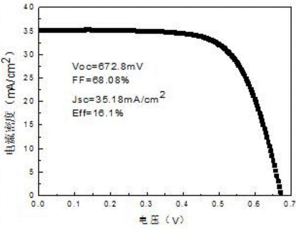
[0024] The structure of a perovskite / silicon heterojunction two-terminal laminated solar cell in the prior art of this embodiment includes, from top to bottom: a metal grid line electrode M1, a transparent electrode T, and a perovskite top cell spacer. Hole transport material layer HTL, perovskite absorption layer, top cell electron transport layer ETL, tunnel junction ITO, silicon heterojunction bottom cell hole selection layer p, passivation layer i, substrate S, passivation layer i, Electron selective layer n and metal back electrode M2.

[0025] The crystalline silicon layer S is n-type polished single crystal silicon.

[0026] The perovskite / silicon heterojunction two-terminal tandem solar cell of this embodiment is prepared by the following method:

[0027] 1. Place the polished Cz silicon wafer substrate with N-type crystal orientation in a PECVD system with high vacuum, and deposit a layer of intrinsic amorphous silicon passivation layer i on the front and back surfa...

Embodiment 2

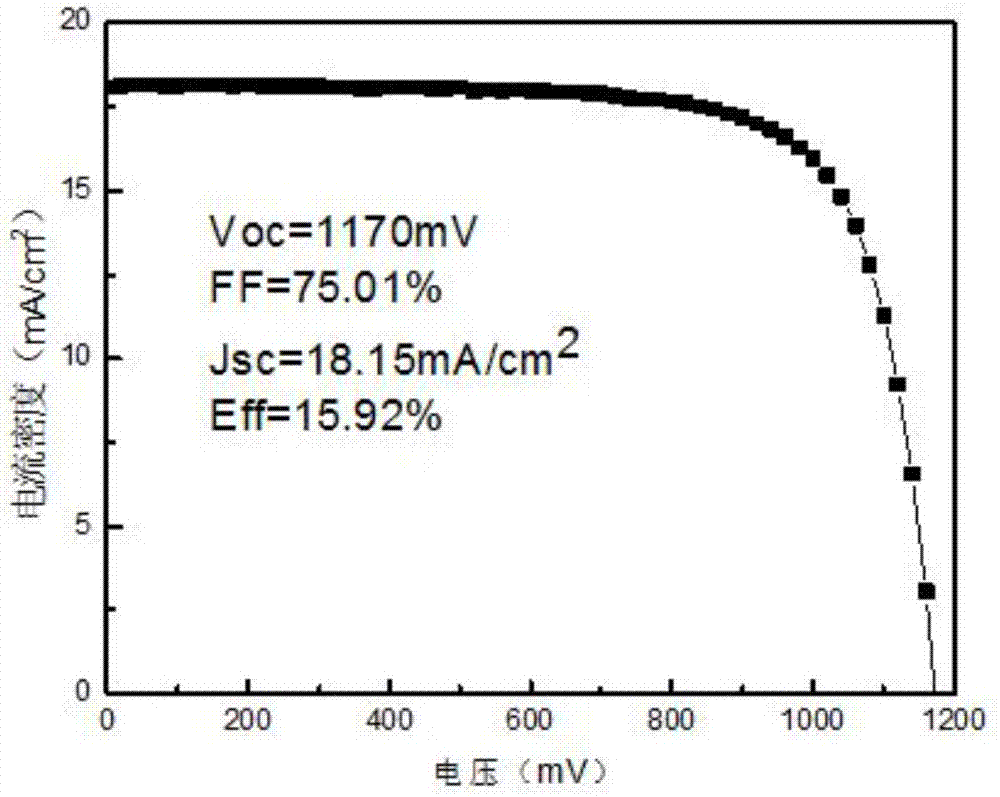
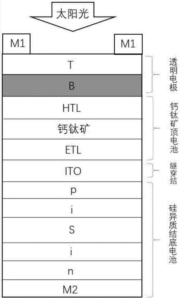
[0036] The structure of a perovskite / silicon heterojunction two-terminal stacked solar cell applying the technology of the present invention in this embodiment is as follows image 3 As shown, it includes from top to bottom: metal grid line electrode M1, transparent electrode T, intermediate protective layer B, perovskite top cell hole transport layer HTL, perovskite absorption layer, top cell electron transport layer ETL, tunnel Through junction ITO, silicon heterojunction bottom cell hole selection layer p, passivation layer i, substrate S, passivation layer i, electron selection layer n and metal back electrode M2.

[0037] The crystalline silicon layer S is n-type polished single crystal silicon.

[0038] The perovskite / silicon heterojunction two-terminal tandem solar cell of this embodiment is prepared by the following method:

[0039] 1. Place the polished Cz silicon wafer substrate with N-type crystal orientation in a PECVD system with high vacuum, and deposit a layer...

Embodiment 3

[0048]The structure of a perovskite / silicon heterojunction two-terminal tandem solar cell in this embodiment is as follows image 3 As shown, it includes from top to bottom: metal grid line electrode M1, transparent electrode T, intermediate protective layer B, perovskite top cell hole transport layer HTL, perovskite absorption layer, top cell electron transport layer ETL, tunnel Through junction ITO, silicon heterojunction bottom cell hole selection layer p, passivation layer i, substrate S, passivation layer i, electron selection layer n and metal back electrode M2.

[0049] The crystalline silicon layer S is n-type polished single crystal silicon.

[0050] The perovskite / silicon heterojunction two-terminal tandem solar cell of this embodiment is prepared by the following method:

[0051] 1. Place the polished Cz silicon wafer substrate with N-type crystal orientation in a PECVD system with high vacuum, and deposit a layer of intrinsic amorphous silicon passivation layer i...


PUM


Abstract

The invention relates to the field of a solar cell, and provides a perovskite/silicon heterojunction two-end laminated solar cell. In the laminated solar cell, the cell with high open voltage and high efficiency is obtained by employing a heterojunction solar cell as a bottom cell, a perovskite solar cell as a top cell and ITO as a tunneling junction and by the matched energy level of a silicon cell and perovskite. By fabricating an intermediate protection layer on a hole transmission layer of the top cell, the laminated solar cell is prevented from being damaged by a subsequent transparent electrode, the structure is prevented from being damaged, the filling factor of the laminated solar cell is improved, and the efficiency is further improved. The preparation method for the material employed by the structure is simple and is easy to implement, and relatively good conversion efficiency can be obtained.

Description

technical field [0001] The invention relates to the technical field of solar cells, in particular to the structural design and realization of a perovskite / silicon heterojunction two-terminal laminated solar cell. Background technique [0002] Due to the advantages of solar photovoltaic power generation, which is safe and reliable, less restricted by geographical factors, and can be easily combined with buildings, it has developed rapidly. If it can be applied to large-scale power generation, it is necessary to reduce production costs and improve the photoelectric conversion efficiency of solar cells. Due to its advantages of high efficiency and low price, low-temperature preparation, high opening voltage, and good stability, silicon heterojunction cells have developed rapidly and have a wide absorption spectrum (300-1200nm), but because of their low utilization rate for short-wavelength and high-energy light absorption And limit the efficiency. Perovskite solar cells have ...

Claims


Application Information

Patent Timeline
IPC IPC(8): H01L51/42H01L51/44
CPCH10K30/10H10K30/00H10K30/30H10K30/81Y02E10/549
Inventor 张晓丹郑翠翠朱世杰任千尚李盛喆魏长春丁毅任慧志黄茜李宝璋赵颖
Owner NANKAI UNIV
Why Eureka
Try Eureka