Hydrothermal preparation method of nickel passivated porous silicon
A technology of porous silicon and silicon wafer, applied in the field of hydrothermal preparation of porous silicon, can solve the problems of complicated experimental process, uneven pore size of porous silicon, narrow application of porous silicon, etc., and achieve the effect of concentrated size distribution and good uniformity
- Summary
- Abstract
- Description
- Claims
- Application Information
AI Technical Summary
Problems solved by technology
Method used
Image
Examples
Embodiment 1
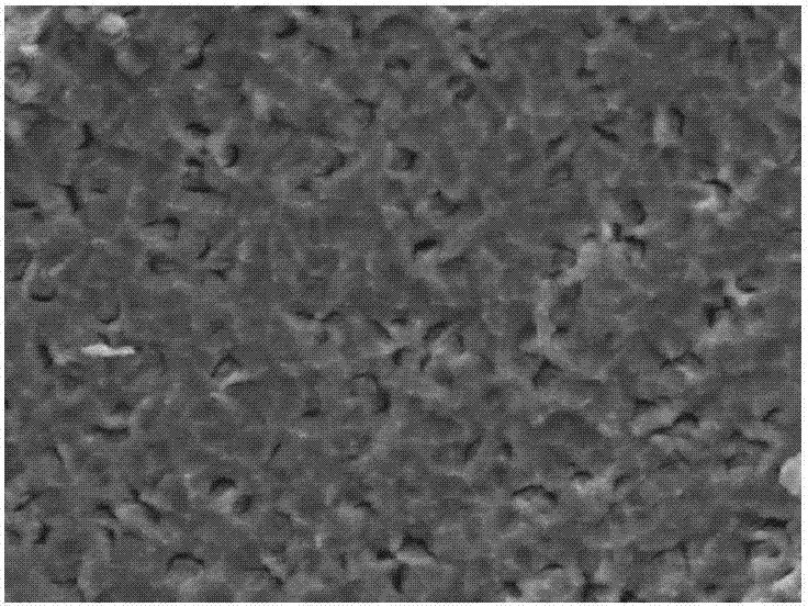
[0038] Cut an n-type single crystal silicon wafer with a crystal plane of and a resistivity of 2-4Ω·cm into a square piece of 1x1cm, soak in acetone and absolute ethanol for 3 minutes each, and rinse with distilled water after the end; use 10 Soak in %HF solution for about 10 minutes, and rinse with distilled water after the end; NH 3 ·H 2 O (28%), H 2 o 2 、H 2 O (volume ratio 1:1:5) mixed solution and HCl (37%), H 2 o 2 、H 2 O (volume ratio 1:1:5) mixed solutions, each soaked for 5min, rinsed with distilled water after the end. The above treated silicon wafer was fixed on the inner lining of the hydrothermal reactor, and then a mixed etching solution was added: 52mL of hydrofluoric acid (40%), 1.1632g of nickel nitrate, 26mL of distilled water and 2mL of absolute ethanol. Seal and heat up, and react at 140° C. for 60 minutes to obtain nickel-passivated porous silicon.
[0039] The morphology of the samples was observed by scanning electron microscope (SEM).
[0040]...
Embodiment 2
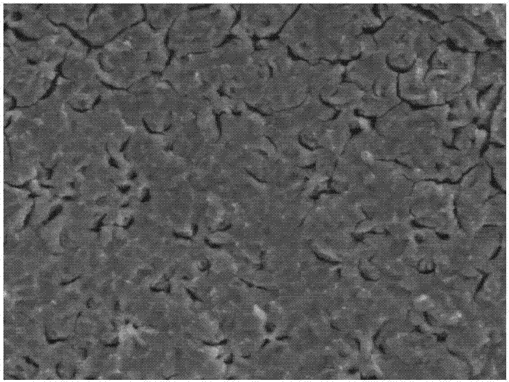
[0042]Other treatment conditions are the same as in Example 1, only the concentration of nickel nitrate in the mixed corrosion solution is increased to 0.2mol / L. The morphology of the samples was also observed with a scanning electron microscope (SEM). Such as figure 2 As shown, compared with the porous silicon prepared in Example 1, the uniformity of the pore structure is reduced.
Embodiment 3
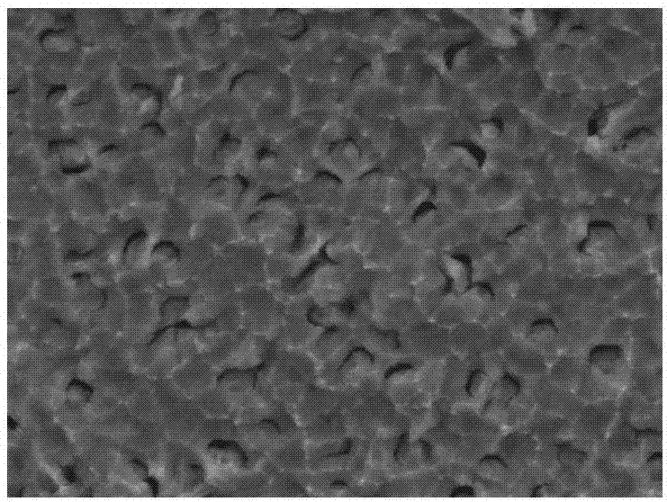
[0044] The other treatment conditions are the same as in Example 1, except that post-annealing treatment is added: the porous silicon is taken out from the etching solution, washed with deionized water, and then directly placed in high-purity nitrogen at 900° C. for 3 hours for annealing.
[0045] Such as image 3 As shown, the size of the post-treated porous silicon increases, and the uniformity is significantly improved.
[0046] The photoluminescence phenomenon of the porous silicon sample prepared in the above-mentioned examples 1 and 2 is tested: the optical fiber test composed of USB2000-FLG fiber optic spectrometer, LS-450 light emitting diode, R400-7 trans probe (Ocean Optics, USA) system. Such as Figure 4 As shown, the luminescence peak of the sample in Example 1 is narrower and the luminescence intensity is higher. The luminescence peak of the sample in Example 2 is wider and weaker than that of the sample in Example 1.
PUM
| Property | Measurement | Unit |
|---|---|---|
| Resistivity | aaaaa | aaaaa |
Abstract
Description
Claims
Application Information


