

Direct band gap modified Ge material based on GeSiC selective epitaxy and preparation method for the same
A selective epitaxy and direct technology, applied in the direction of electrical components, circuits, semiconductor devices, etc., can solve the problems of high strength, difficult to achieve 2.4GPa biaxial stress, and difficult process realization, so as to achieve high working speed and enhanced spontaneous radiation efficiency , good frequency characteristics
- Summary
- Abstract
- Description
- Claims
- Application Information
AI Technical Summary
Problems solved by technology
Method used
Image

Examples
Embodiment 1
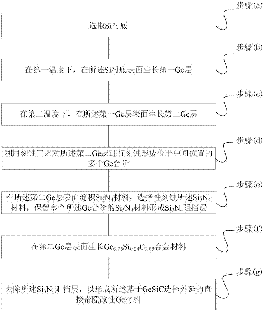
[0053] See figure 2 , figure 2 It is a process flow chart of a direct band gap modification of Ge material based on GeSiC selective epitaxy provided by an embodiment of the present invention. The method includes the following steps:
[0054] Step a, select Si substrate;
[0055] Step b, at a first temperature, growing a first Ge layer on the surface of the Si substrate;
[0056] Step c, at a second temperature, growing a second Ge layer on the surface of the first Ge layer;
[0057] Step d, using an etching process to etch the second Ge layer to form a plurality of Ge steps located in the middle position;
[0058] Step e, depositing Si on the surface of the second Ge layer 3 N 4 Material, selectively etch the Si 3 N 4 Material, Si that retains multiple Ge steps 3 N 4 Material forms Si 3 N 4 Barrier layer
[0059] Step f, using chemical vapor deposition to grow Ge on the surface of the second Ge layer 0.73 Si 0.24 C 0.03 alloy;
[0060] Step g, remove the Si 3 N 4 Barrier layer to form ...
Embodiment 2
[0077] See Figure 5a-Figure 5i , Figure 5a-Figure 5i This is a process schematic diagram of a direct bandgap modification of Ge material based on GeSiC selective epitaxy provided by an embodiment of the present invention. On the basis of the foregoing embodiment, this embodiment will introduce the process flow of the present invention in more detail. The method includes:
[0078] S101. The substrate is selected. Such as Figure 5a As shown, the Si (001) substrate sheet 201 is selected as the original material;
[0079] S102, epitaxial layer growth:
[0080] S1021. Using the CVD method, grow an n-type Ge(001) film on the substrate with a low and high temperature two-part method, with a doping concentration of 1×10 16 ~5×10 16 cm -3 .
[0081] S1022, such as Figure 5b As shown, a 40nm thick "low temperature" Ge (LT-Ge) layer 202 is grown at 275-325°C. Most of the relaxation of the elastic stress occurs in the low-temperature Ge layer less than 10 nanometers, but in order to avoid t...
PUM
 Abstract
Description
Claims
Application Information