A kind of preparation transparent bi 2 se 3 thin film method

A thin-film and transparent technology, which is applied in the field of preparing transparent Bi2Se3 thin films, can solve the problems of low deposition rate, high energy consumption, and flammable residual gas, and achieve high magnetron sputtering efficiency, low preparation cost, and good repeatability Effect

Active Publication Date: 2019-12-27
SOUTHWEST JIAOTONG UNIV
View PDF4 Cites 0 Cited by
  • Summary
  • Abstract
  • Description
  • Claims
  • Application Information

AI Technical Summary

Problems solved by technology

However, MBE technology requires high-precision vacuum pumps, expensive equipment, large energy consumption, and high cost
However, the deposition rate of CVD technology is low, and the residual gas participating in the deposition is flammable, explosive or toxic, and measures to prevent environmental pollution need to be taken; and there are also requirements for corrosion resistance of equipment

Method used


Image

  • A kind of preparation transparent bi  <sub>2</sub> se  <sub>3</sub> thin film method
  • A kind of preparation transparent bi  <sub>2</sub> se  <sub>3</sub> thin film method
  • A kind of preparation transparent bi  <sub>2</sub> se  <sub>3</sub> thin film method

Examples


Embodiment 1

[0025] A preparation of transparent Bi 2 Se 3 A thin film method comprising the steps of:

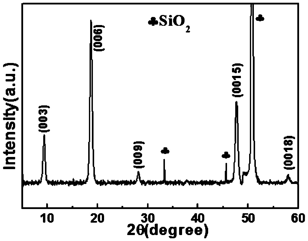
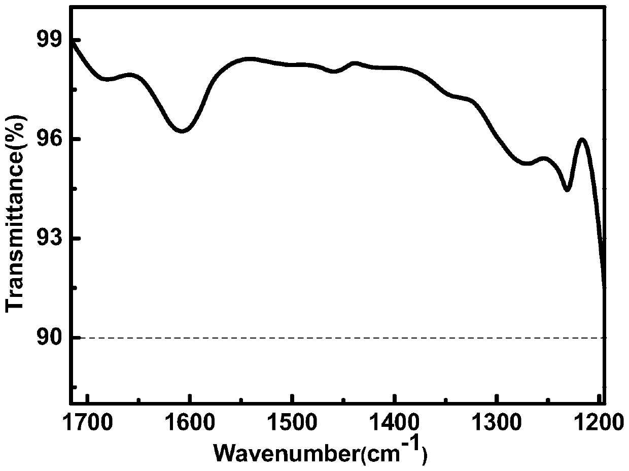
[0026] a. Sputtering deposition: select quartz (SiO 2 ) substrate or sapphire (Al 2 o 3 ) substrate as the substrate for magnetron sputtering, select Bi with a purity of 99.999% 2 Se 3 The material is used as the target material of magnetron sputtering, and a layer of Bi is deposited on the substrate by sputtering 2 Se 3 film;

[0027] The process conditions of sputtering deposition are: the distance from the target to the substrate is 7cm, and the air pressure in the vacuum chamber is less than 2×10 -4 Pa, and then feed argon with a purity of 99.995% as the working gas; the gas pressure during sputtering is 0.5 Pa, the substrate temperature is 330° C., the sputtering power is 70 W, and the sputtering time is 3 seconds.

[0028] b. Post-annealing treatment: deposit Bi with step a 2 Se 3 The substrate of the film and selenium balls with a particle size of 0.6mm-1.2mm are seal...

Embodiment 2

[0035] A preparation of transparent Bi 2 Se 3 A thin film method comprising the steps of:

[0036] a. Sputtering deposition: select sapphire (Al 2 o 3 ) substrate as the substrate for magnetron sputtering, Bi with a purity of 99.999% was selected 2 Se 3 The material is used as the target material of magnetron sputtering, and a layer of Bi is deposited on the substrate by sputtering 2 Se 3 film;

[0037] The process conditions of sputtering deposition are: the distance from the target to the substrate is 5cm, and the air pressure in the vacuum chamber is less than 2×10 -4 Pa, and then feed argon with a purity of 99.995% as the working gas; the gas pressure during sputtering is 0.45Pa, the substrate temperature is 350°C, the sputtering power is 60W, and the sputtering time is 5 seconds.

[0038] b. Post-annealing treatment: deposit Bi with step a 2 Se 3 The substrate of the film and the selenium balls with a particle size of 0.9 mm are sealed together with an air pressu...

Embodiment 3

[0045] A preparation of transparent Bi 2 Se 3 A thin film method comprising the steps of:

[0046] a. Sputtering deposition: select quartz (SiO 2 ) substrate as the substrate for magnetron sputtering, select Bi with a purity of 99.999% 2 Se 3 The material is used as the target material of magnetron sputtering, and a layer of Bi is deposited on the substrate by sputtering 2 Se 3 film;

[0047] The process conditions of sputtering deposition are: the distance from the target to the substrate is 6cm, and the air pressure in the vacuum chamber is less than 2×10 -4 Pa, and then feed argon with a purity of 99.995% as the working gas; the gas pressure during sputtering is 0.35Pa, the substrate temperature is 380°C, the sputtering power is 55W, and the sputtering time is 10 seconds.

[0048] b. Post-annealing treatment: deposit Bi with step a 2 Se 3 The substrate of the film and selenium balls with a particle size of 1.0 mm are sealed together with an air pressure of less th...


PUM


Abstract

A preparation of transparent Bi 2 Se 3 The method for thin film comprises the following steps: a, sputter deposition: choose quartz (SiO 2 ) substrate or sapphire (Al 2 o 3 ) substrate as the substrate for magnetron sputtering, select Bi with a purity of 99.999% 2 Se 3 The material is used as the target material of magnetron sputtering, and a layer of Bi is deposited on the substrate by sputtering 2 Se 3 Thin film; b, post-annealing treatment: the a step is deposited with Bi 2 Se 3 The substrate of the film and selenium balls with a particle size of 0.6mm-1.2mm are sealed together with an air pressure of less than 1×10 ‑2 Pa vacuum quartz tube, then put the vacuum quartz tube in a tube furnace, and carry out post-annealing treatment under the protective atmosphere of argon to obtain transparent Bi 2 Se 3 film. This method can prepare large-area Bi with good light transmission properties. 2 Se 3 The thin film has simple preparation process, low energy consumption, low cost, high efficiency and good repeatability, and is suitable for industrial production.

Description

technical field [0001] The invention relates to a method for preparing transparent Bi 2 Se 3 Thin film method, especially related to the preparation of transparent Bi by magnetron sputtering 2 Se 3 thin film method. Background technique [0002] Bi 2 Se 3 The transparent film belongs to the VA-VIA group of direct band gap inorganic semiconductors. It has narrow band gap, stable performance, good photoelectric conversion performance, and it has remarkable third-order nonlinear optical characteristics, short response time and large nonlinear The optical coefficient can be used as a nonlinear optical device. Transparent Bi 2 Se 3 Thin films have broad application prospects in high-performance optoelectronic devices (all-optical switches, photodetectors, terahertz lasers, waveguides, transparent electrodes) and light processing. Various methods have been used to prepare transparent Bi 2 Se 3 Thin films such as molecular beam epitaxy (MBE) and chemical vapor deposition...

Claims


Application Information

Patent Timeline
Patent Type & Authority Patents(China)
IPC IPC(8): C23C14/06C23C14/35C23C14/58C30B23/00C30B29/46C30B33/02
Inventor 羊新胜刘悦赵可雷鸣赵勇
Owner SOUTHWEST JIAOTONG UNIV
Why Eureka
Try Eureka