Post-treatment method of copper indium gallium selenide absorbing layer and solar cell preparation method based on it

A technology of copper indium gallium selenide and thin-film solar cells, which is applied in the field of new energy, can solve the problems of affecting the characteristics of CdS/CIGS heterojunction, the increase of CdS/CIGS interface states, and the inability to form effective connections, so as to achieve simple and reliable equipment and promote The effect of depth expansion and low cost

Active Publication Date: 2020-06-30
SHANGHAI INST OF MICROSYSTEM & INFORMATION TECH CHINESE ACAD OF SCI
View PDF7 Cites 0 Cited by
  • Summary
  • Abstract
  • Description
  • Claims
  • Application Information

AI Technical Summary

Problems solved by technology

[0005] However, since the non-vacuum method is used to deposit the CdS buffer layer, it cannot form an effective connection with the vacuum preparation process of the CIGS absorber layer commonly used in laboratories and industries. In the process of taking out and storing the CIGS absorber layer Among them, the CIGS absorber layer will increase the CdS / CIGS interface state due to surface contamination and oxidation, resulting in enhanced recombination at the interface, thereby affecting the heterojunction characteristics of CdS / CIGS, and ultimately affecting the battery performance, especially the open circuit voltage V OC and fill factor FF adversely affect

Method used


Image

  • Post-treatment method of copper indium gallium selenide absorbing layer and solar cell preparation method based on it
  • Post-treatment method of copper indium gallium selenide absorbing layer and solar cell preparation method based on it
  • Post-treatment method of copper indium gallium selenide absorbing layer and solar cell preparation method based on it

Examples


Embodiment 1

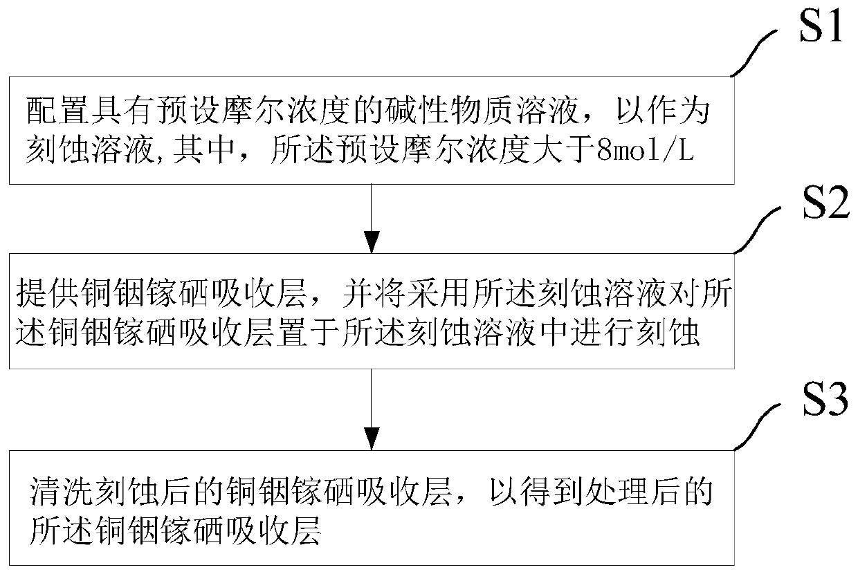
[0061] Such as Figure 1~6 As shown, the present invention provides a post-treatment method for the absorbing layer of a copper indium gallium selenide thin film solar cell, comprising the steps of:

[0062] 1) configuring an alkaline substance solution with a preset molar concentration as an etching solution, wherein the preset molar concentration is greater than 8 mol / L;

[0063] 2) providing a copper indium gallium selenide absorption layer, and using the etching solution to etch the copper indium gallium selenide absorption layer, so as to modify the surface of the copper indium gallium selenide absorption layer;

[0064] 3) Cleaning the etched CIGS absorption layer to obtain the CIGS absorption layer after treatment.

[0065] The post-treatment method of the absorption layer of the copper indium gallium selenium thin film solar cell of the present invention will be described in detail below in conjunction with specific drawings.

[0066] Such as figure 1 As shown in S1...

Embodiment 2

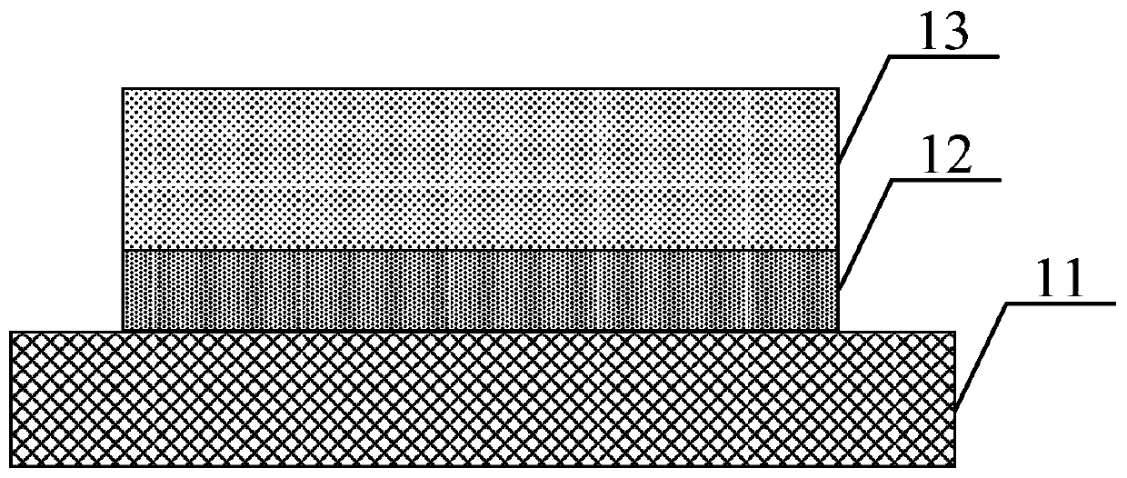
[0106] This embodiment provides a method for preparing a copper indium gallium selenide thin film solar cell, comprising the following steps:

[0107] 1) providing a substrate 11, and forming a first electrode layer 12 on the substrate;

[0108] 2) forming a copper indium gallium selenide absorption layer 13 on the surface of the first electrode layer 12;

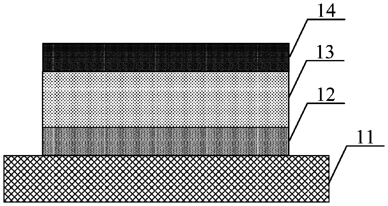
[0109] 3) post-processing the CIGS absorption layer 13 by any one of the methods in the embodiment;

[0110] 4) forming a window layer 15 on the surface of the obtained structure in step 3);

[0111] 5) Forming the second electrode layer 16 on the surface of the window layer 15 .

[0112] Specifically, when the post-processing method of forming a buffer layer of the absorbing layer is adopted, the buffer layer 14 (such as a CdS buffer layer) will be formed on the surface of the copper indium gallium selenide absorbing layer 13, and the window layer 15 is formed on The buffer layer 14 surface.

[0113] As an example, the...

Embodiment 3

[0124] This embodiment three provides another method for preparing a copper indium gallium selenide thin-film solar cell. The difference between this embodiment three and embodiment two is:

[0125] In step 2-2), a batch of CIGS absorbing layers with [Cu] / [In+Ga] of about 0.92 were prepared, with a thickness of about 1.2 μm. In addition, the prepared CuInGaSe absorbing layers were stored in dry Cabinet for 30min (vacuum degree is about 10 2 Pa level), 0.5 days in the air, 1 day in the air, 2 days in the air.

[0126] It should be noted that, compared with the copper indium gallium selenide thin film solar cell prepared by the above method of this embodiment, the open circuit voltage can be increased by about 30mV, and the fill factor can be increased by 3.6%. , the absolute value of the battery conversion efficiency increases by 1.2%. In addition, if Figure 6 As shown, it provides the copper indium gallium selenide thin film solar cell prepared by the method of the present ...


PUM

PropertyMeasurementUnit
thicknessaaaaaaaaaa
thicknessaaaaaaaaaa
thicknessaaaaaaaaaa

Abstract

The invention provides a post-processing method for a copper-indium-gallium-selenium thin-film solar cell absorber layer and a preparation method of a solar cell based on the same. The post-processingmethod comprises: an etching solution having an alkaline matter with a preset molar concentration is prepared, wherein the preset molar concentration is larger than 8mol / L; a copper-indium-gallium-selenium absorber layer is provided and the copper-indium-gallium-selenium absorber layer is etched by using the etching solution, so that surface modification is carried out on the copper-indium-gallium-selenium absorber layer; and the etched copper-indium-gallium-selenium absorber layer is cleaned to obtain a processed copper-indium-gallium-selenium absorber layer. According to the method providedby the invention, the surface interface of the copper-indium-gallium-selenium absorber layer is modified, the surface characteristics of the copper-indium-gallium-selenium absorber layer are optimized, and longitudinal deep extension of the shallow buried PN junction is promoted; composition of carriers at the buffer layer / absorber layer interface is reduced, so that the open-circuit voltage of the copper-indium-gallium-selenium thin-film solar cell is increased, the filler factor is improved, and the absolute value of the battery conversion efficiency is increased.

Description

technical field [0001] The invention belongs to the technical field of new energy, and in particular relates to a post-treatment method of an absorbing layer of a copper indium gallium selenium thin film solar cell and a solar cell preparation method based thereon. Background technique [0002] copper indium gallium selenide [Cu(In,Ga)Se 2 , CIGS] thin-film solar cells have strong competitiveness in the industrialization of low-cost, high-efficiency solar cells due to their good stability, high photoelectric conversion efficiency, and the replaceability of the rare element In, and can be prepared into flexible cells. , thus providing an important opportunity for the expansion of the global diversified photovoltaic market. [0003] In 2016, the 0.5cm 2 The efficiency of small-area copper indium gallium selenide thin film solar cells has reached 22.6%, making it the most efficient type of single junction thin film solar cells. At present, the highest module efficiency certi...

Claims


Application Information

Patent Timeline
Patent Type & Authority Patents(China)
IPC IPC(8): H01L31/0392H01L31/0445H01L31/18
CPCY02E10/50Y02P70/50
Inventor 王宪韩安军韦小庆黄勇亮刘正新
Owner SHANGHAI INST OF MICROSYSTEM & INFORMATION TECH CHINESE ACAD OF SCI
Why Eureka
Try Eureka