Tin selenide thin film transverse thermoelectric effect-based light and heat detector
A thermal detector and transverse thermoelectric technology, which is applied in the manufacture/processing of thermoelectric devices, materials for lead-out wires of thermoelectric devices, ion implantation plating, etc., can solve the problems of detector performance improvement, high cost, detection element preparation process, etc. cumbersome process and other issues, to achieve the effect of low cost, simple structure, and simple preparation process
- Summary
- Abstract
- Description
- Claims
- Application Information
AI Technical Summary
Problems solved by technology
Method used
Image
Examples
Embodiment 1
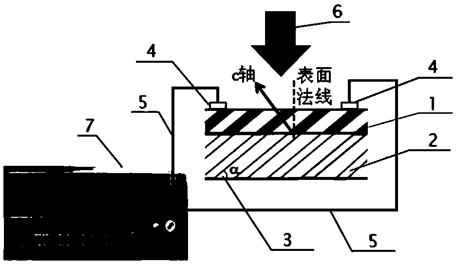
[0031] Such as figure 1 Shown, the present invention is based on the photoelectricity of tin selenide thin film lateral pyroelectric effect, thermal detector comprises detection element, metal electrode 4 and metal lead 5, and detection element comprises oxide single crystal substrate 2 and is deposited on oxide single crystal substrate The tin selenide film 1 on the 2 has two metal electrodes 4 symmetrically arranged on the upper surface of the tin selenide film 1, and the two metal electrodes 4 are connected to the input terminal of the voltmeter 7 through the metal lead 5. Use the probe beam 6 to irradiate the surface of the detector, and use the voltmeter 7 to record the change of its voltage signal.
[0032] The preparation method of the light and heat detector comprises the following steps:
[0033] (1) Preparation of detection element
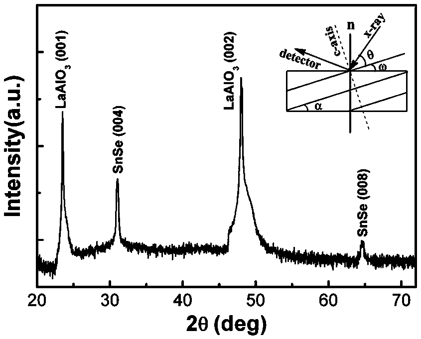
[0034] LaAlO tilted at c-axis 10° 3 Prepare a layer of tin selenide film with a thickness of 100nm and c-axis oblique growth on the ...
Embodiment 2
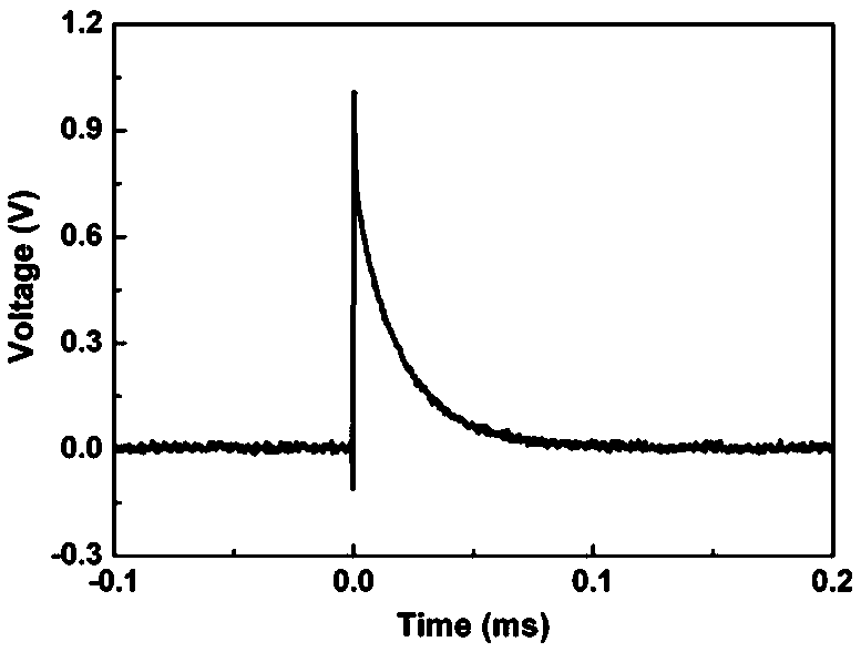
[0041] The surface of the detector prepared in embodiment 1 is irradiated by pulsed light with a wavelength of 308nm, the output voltage signal is recorded with an oscilloscope, and the detector output voltage-time response curve is drawn, such as image 3 shown.
[0042] Depend on image 3 It can be seen that when the pulse light energy irradiated on the film is 27.5 mJ (energy density 0.55mJ / mm 2 , spot area 5×10mm 2 ), the amplitude of the output voltage signal is 1.1V, and the detection sensitivity is 40 mV / mJ.
Embodiment 3
[0044] The continuous laser light with wavelength of 532nm and 808nm is used to irradiate the center position between the two electrodes on the surface of the detector prepared in Example 1 respectively, record the output voltage signal with a voltmeter, and draw the detector output voltage-time response curve, as Figure 4 shown. Depend on Figure 4 It can be seen that when the irradiation laser power is 50mW, the amplitudes of the two output voltage signals are 70mV and 46mV, respectively, and the corresponding detection sensitivities are 1.4V / W and 0.92V / W, which are much higher than other oxides designed based on the transverse thermoelectric effect. The detection sensitivity of the object photodetector.
PUM
| Property | Measurement | Unit |
|---|---|---|
| thickness | aaaaa | aaaaa |
| diameter | aaaaa | aaaaa |
| thickness | aaaaa | aaaaa |
Abstract
Description
Claims
Application Information


