Supercharge Your Innovation With Domain-Expert AI Agents!

Ka-band SiGe BiCMOS radio frequency power amplifier

A radio frequency power and power amplifier circuit technology, applied in power amplifiers, radio frequency amplifiers, amplifiers, etc., can solve the problems of poor current driving ability, difficult integration, poor performance of on-chip passive devices, etc. Effects of integration, high eigenfrequency and noise characteristics

Inactive Publication Date: 2018-02-02
MIANYANG XINYANG INTPROP CO LTD
View PDF0 Cites 2 Cited by
  • Summary
  • Abstract
  • Description
  • Claims
  • Application Information

AI Technical Summary

Problems solved by technology

But at the same time, it also brings some difficulties to the RF power amplifier, such as the breakdown voltage of the oxide layer of the CMOS device is too low, the current driving ability is poor, and the substrate coupling is serious, etc.
In addition, the performance of on-chip passive devices is poor, especially the Q value of on-chip inductors is too low, which seriously affects the performance of power amplifiers. Therefore, components such as inductors often use off-chip methods, that is, the passive devices of RF power amplifiers implemented by existing CMOS processes such as Inductors and active devices such as CMOS devices often cannot be formed on the same chip, that is, the full chip integration of the entire RF power amplifier cannot be realized
Since the inductor needs to be manufactured off-chip, compared with a fully integrated RF power amplifier in which all components are integrated on the same chip, the cost of the existing RF power amplifier will be high and the application is inconvenient
[0004] except as figure 1 In addition to the RF power amplifiers realized by the existing CMOS process shown, the existing RF power amplifiers are also implemented by using gallium arsenide heterojunction bipolar transistors. Although GaAs HBTs have better performance, they cannot be integrated with silicon processes; In the field of semiconductor manufacturing, only silicon-based devices can achieve large-scale manufacturing, and GaAs cannot be integrated with silicon processes, so the cost is very high
[0005] In response to the urgent demand for general-purpose modules such as Ka-band millimeter-wave power amplifiers in communication systems, on the one hand, the existing industry-widely used millimeter-wave power amplifier chips based on III-V semiconductor technology are expensive, which limits their large-scale use
At the same time, III-V chips have disadvantages such as large size, complicated process and difficulty in integration.

Method used


Image

  • Ka-band SiGe BiCMOS radio frequency power amplifier
  • Ka-band SiGe BiCMOS radio frequency power amplifier
  • Ka-band SiGe BiCMOS radio frequency power amplifier

Examples


Embodiment 1

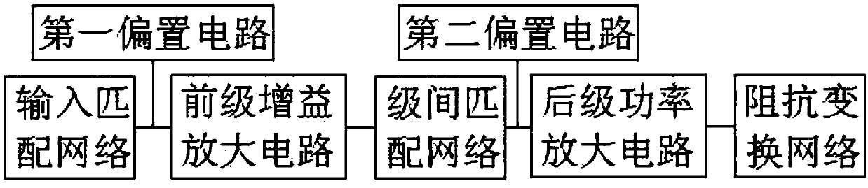
[0028] Such as figure 2 A Ka-band SiGe BiCMOS RF power amplifier is shown, which is used in fully integrated RF circuits, communication SOC and other fields, including input matching network, pre-stage gain amplifier circuit, inter-stage matching network, post-stage power amplifier circuit and impedance transformation network, which in turn are connected;

[0029] Both the pre-stage gain amplifier circuit and the rear-stage power amplifier circuit include SiGe BiCMOS;

[0030] The input terminals of the front-stage gain amplifier circuit and the rear-stage power amplifier circuit are respectively connected with a first bias circuit and a second bias circuit.

[0031] The above-mentioned circuit can have good power output and gain by means of two stages with different emphases. And because the SiGe transistor has a heterojunction structure with a wide-bandgap emitter region, the carrier injection efficiency of the emitter junction is greatly improved, the carrier drift movem...

Embodiment 2

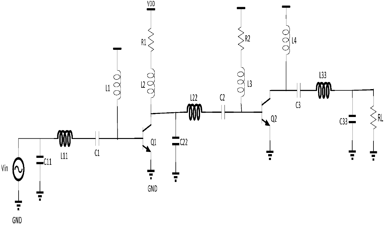
[0033] This embodiment is optimized on the basis of the above embodiments, that is, the circuit structures of the input matching network, the interstage matching network and the impedance transformation network are the same. The three circuits adopt the same circuit structure, which can not only improve the consistency, but also ensure the stability of the circuit. Specifically, such as image 3 As shown, it can adopt the following structure, that is, it includes a first inductor and a first capacitor connected in series at the input end, and a second capacitor connected at the input end and the other end is grounded.

[0034] Such as figure 1 As shown, the input matching network includes inductor L11, capacitor C1, and capacitor C11, the interstage matching network includes inductor L22, capacitor C2, and capacitor C22, and the impedance transformation network includes inductor L33, capacitor C3, and capacitor 33. The impedance transformation network includes an inductor L3...

Embodiment 3

[0037] On the basis of the above examples, if image 3 As shown, the front-stage gain amplifying circuit, the post-stage power amplifying circuit, the first bias circuit, and the second bias circuit can adopt the following structures.

[0038]The first bias circuit includes a second inductance L1, and the two ends of the second inductance are respectively connected to the input terminal of the pre-stage gain amplifier circuit and the power supply.

[0039] The second bias circuit includes a second resistor R2 and a fifth inductor L3 connected in series with one end connected to the power supply and the other end connected to the input end of the subsequent power amplifier circuit. With the bias circuit of this structure, the inductance in the bias circuit participates in matching and impedance transformation, which can effectively reduce the use of original components, reduce the cost, reduce the area, and have reliable performance.

[0040] The pre-stage gain amplifier circu...


PUM


Abstract

The present invention discloses a Ka-band SiGe BiCMOS radio frequency power amplifier. The radio frequency power amplifier comprises an input matching network, a front stage gain amplification circuit, an inter-stage matching network, a post stage power amplification circuit and an impedance transformation network which are connected sequentially; the front stage gain amplification circuit and thepost stage power amplification circuit comprise SiGe BiCMOS; the input ends of the front stage gain amplification circuit and the post stage power amplification circuit are respectively connected with a first biasing circuit and a second biasing circuit. The employment of two-stage amplification and the SiGe BiCMOS as an amplifier tube is able to meet the high efficiency to achieve sufficient gain and output power to solve the problems such as poor performance of CMOS, and high cost and large volume of III-V semiconductors. The radio frequency power amplifier has high characteristic frequencyand noise characteristics, and is more conducive to integration.

Description

technical field [0001] The invention relates to the field of radio frequency power amplifiers, in particular to a Ka-band SiGe BiCMOS radio frequency power amplifier. Background technique [0002] The radio frequency power amplifier is an indispensable and important part of the wireless transmitter. It is mainly used to amplify the power of the modulated signal of the transmitter in the wireless communication to meet the power demand of the radio frequency signal of the wireless communication. Its working bandwidth, output Performances such as power and additional efficiency seriously affect the quality of wireless communication systems. [0003] Such as figure 1 As mentioned above, the existing radio frequency power amplifier is realized by using NMOS devices, that is, it can be realized by using CMOS technology. With the advancement of CMOS technology, the high-frequency performance of CMOS devices has been improved, which has also improved the high-frequency performance...

Claims


Application Information

Patent Timeline
Patent Type & Authority Applications(China)
IPC IPC(8): H03F3/193H03F3/21H03F3/24
CPCH03F1/26H03F1/565H03F3/193H03F3/21H03F3/211H03F3/245H03F2200/451H03G3/3036
Inventor 龚平
Owner MIANYANG XINYANG INTPROP CO LTD
Features
  • R&D
  • Intellectual Property
  • Life Sciences
  • Materials
  • Tech Scout
  • Unparalleled Data Quality
  • Higher Quality Content
  • 60% Fewer Hallucinations
Learn More