Semiconductor device, method for making the same, and electronic device

A manufacturing method and semiconductor technology, applied in the fields of semiconductor devices, semiconductor/solid-state device manufacturing, electric solid-state devices, etc., can solve the problems of device performance degradation and poor interface quality, etc.

Active Publication Date: 2021-04-23
SEMICON MFG SOUTH CHINA CORP +2
View PDF4 Cites 0 Cited by
  • Summary
  • Abstract
  • Description
  • Claims
  • Application Information

AI Technical Summary

Problems solved by technology

However, in the current multi-IO device (multi-IO device) manufacturing process, the gate oxide layer of low-voltage devices is mostly formed by ALD (atomic layer deposition), CVD (chemical vapor deposition) and other processes, and the interface quality is poor, resulting in poor device performance. decline

Method used


Image

  • Semiconductor device, method for making the same, and electronic device
  • Semiconductor device, method for making the same, and electronic device
  • Semiconductor device, method for making the same, and electronic device

Examples


Embodiment 1

[0049] The following will refer to Figure 3A ~ Figure 3I A method for fabricating a semiconductor device according to an embodiment of the present invention will be described in detail.

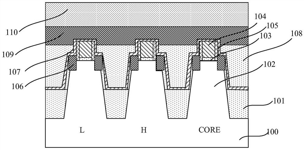
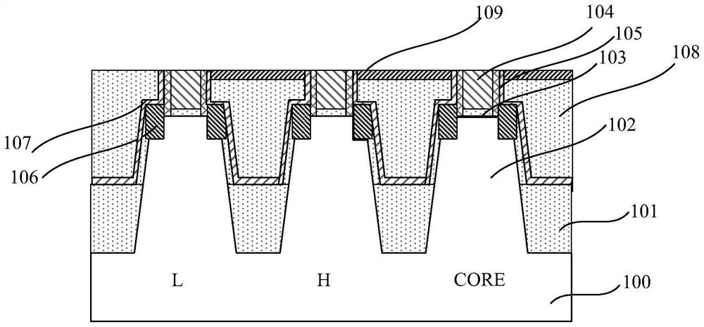
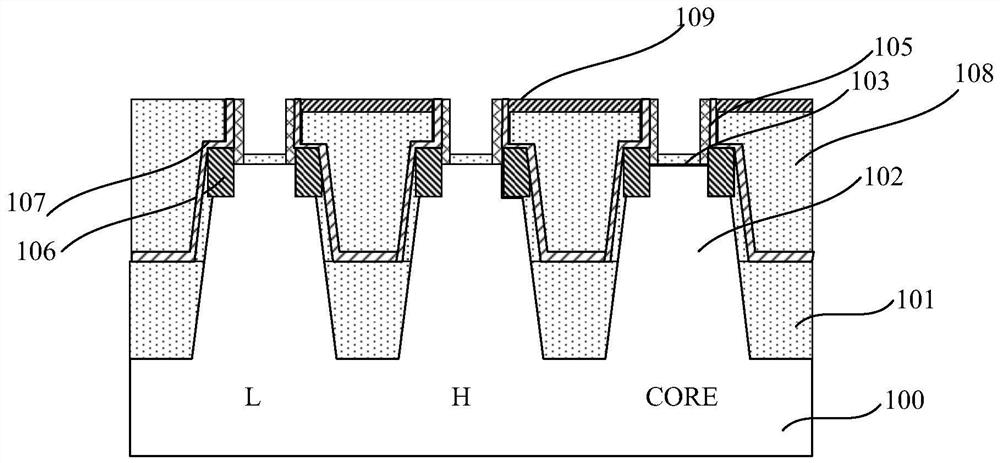
[0050] First, if Figure 3A As shown, a semiconductor substrate 300 is provided. The semiconductor substrate 300 includes a low-voltage device region L, a high-voltage device region H and a core device region CORE. The low-voltage device region L, the high-voltage device region H and the core device region CORE are separated by an isolation structure 301. Fins 302 are formed on the low-voltage device region L, the high-voltage device region H and the core device region CORE, and dummy gate structures and source / drain electrodes 306 located on both sides of the dummy gate structures are formed on the fins 302 . An etching stop layer 307 and an interlayer dielectric layer covering or surrounding the dummy gate structure are also formed on the semiconductor substrate 300 .

[0051] Wherein, t...

Embodiment 2

[0081] The present invention also provides a semiconductor device fabricated by the above method, such as Figure 4 As shown, the semiconductor device includes: a semiconductor substrate 400, the semiconductor substrate 400 includes a low voltage device region L, a high voltage device region H and a core device region core, in the low voltage device region L, high voltage device region H and core device A gate stack and source and drain electrodes 408 located on both sides of the gate stack are formed on the semiconductor substrate in the region core, wherein the gate stack located in the low-voltage device region L includes a gate oxide layer 403 , a high-K material layer 406 and a metal gate (not shown), the gate stack located in the high-voltage device region H includes a gate oxide layer 403, an additional oxide layer 404, a high-K material layer 406 and a metal gate ( not shown), the gate stack located in the core device region includes an interface layer 405, a high-K ma...

Embodiment 3

[0091] Still another embodiment of the present invention provides an electronic device, including a semiconductor device and an electronic component connected to the semiconductor device. Wherein, the semiconductor device includes: a semiconductor substrate, the semiconductor substrate includes a low-voltage device region, a high-voltage device region, and a core device region, and gates are formed on the semiconductor substrate of the low-voltage device region, high-voltage device region, and core device region. pole stack and source and drain located on both sides of the gate stack, wherein the gate stack located in the low-voltage device region includes a gate oxide layer, a high-K material layer and a metal gate, and is located in the The gate stack in the high-voltage device region includes a gate oxide layer, an additional oxide layer, a high-K material layer, and a metal gate, and the gate stack in the core device area includes an interface layer, a high-K material layer...


PUM


Abstract

The invention provides a semiconductor device, a manufacturing method thereof, and an electronic device. The manufacturing method includes: providing a semiconductor substrate, the semiconductor substrate including a low-voltage device area, a high-voltage device area, and a core device area. Forming a dummy gate oxide layer and a dummy gate in the region and the core device region, and an interlayer dielectric layer surrounding the dummy gate oxide layer and the dummy gate; removing the dummy gate in the high-voltage device region to form a first opening, and forming an additional oxide layer on the dummy gate oxide layer in the first opening; removing the dummy gates in the low voltage device region and the core device region to respectively form a second opening and a third opening; removing the dummy gate in the third opening an oxide layer, and form an interface layer in the third opening; form a high-K material layer and a metal gate in the first, second and third openings. The fabrication method can improve device performance. The semiconductor device and electronic device have high performance.

Description

technical field [0001] The present invention relates to the technical field of semiconductors, in particular to a semiconductor device, a manufacturing method thereof, and an electronic device. Background technique [0002] With the development of semiconductor process technology, the critical dimensions of semiconductor devices such as MOSFETs (Metal Oxide Semiconductor Field Effect Transistors) are continuously shrinking, and at the same time, the short channel effect (SCE) is becoming more and more serious. The FinFET (Fin Field Effect Transistor) device can shrink the device to a technology node of 20nm or below due to its good gate control ability on the channel charge. At the same time, in order to better overcome problems such as short channel effects, the post-high K / metal gate process and the replacement gate process are known as common processes for 14nm and below technology nodes. [0003] In practical applications, multi-IO devices (multi-IO devices) are require...

Claims


Application Information

Patent Timeline
Patent Type & Authority Patents(China)
IPC IPC(8): H01L27/088H01L21/8234
CPCH01L21/823431H01L21/823462H01L27/0886
Inventor 周飞
Owner SEMICON MFG SOUTH CHINA CORP
Why Eureka
Try Eureka