Wafer bonding structure and preparation method thereof

A wafer and bonding technology, used in semiconductor/solid-state device manufacturing, electrical components, circuits, etc., can solve the problems of high porosity and low bonding strength, and achieve the effect of high bonding strength, improved strength, and reduced bubbles

Pending Publication Date: 2018-02-27
GUILIN UNIV OF ELECTRONIC TECH
View PDF0 Cites 5 Cited by
  • Summary
  • Abstract
  • Description
  • Claims
  • Application Information

AI Technical Summary

Problems solved by technology

[0006] The technical problem to be solved by the present invention is the technical problem of high porosity and low bonding strength existing in the prior art. It provides

Method used


Image

  • Wafer bonding structure and preparation method thereof
  • Wafer bonding structure and preparation method thereof
  • Wafer bonding structure and preparation method thereof

Examples


Embodiment 1

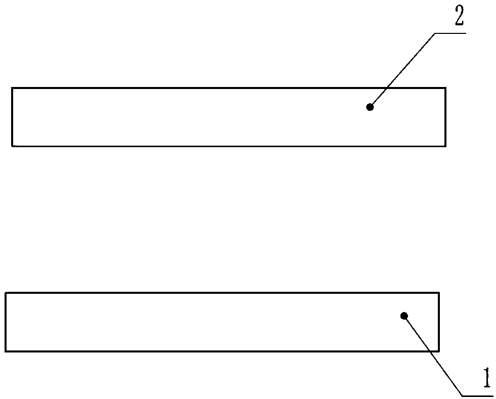
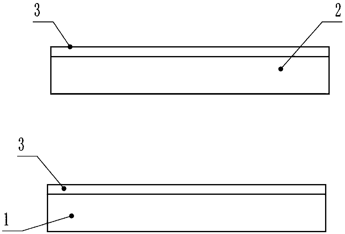
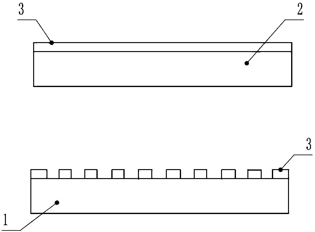
[0049] Such as figure 1 As shown, this embodiment provides a structure of bonded wafers, including a first wafer 1 and a second wafer 2, the first wafer 1 is located at the bottom layer, the top of the first wafer 1 is an intermediate layer, and the intermediate layer It includes a gas channel 9 and an aluminum oxide layer 8, and the second wafer 2 is above the intermediate layer; the gas channel 9 is a groove-shaped gas channel with equal intervals formed by etching with a mixed gas.

[0050] The preparation method of the bonded wafer structure comprises the following steps:

[0051] A. Both the first wafer 1 and the second wafer 2 are cleaned and dried; RCA wet chemical cleaning method is used for cleaning, and the cleaning solution used in the RCA wet chemical cleaning method includes a mixed solution of organic solvent, sulfuric acid and hydrogen peroxide And a mixed solution of ammonia, hydrogen peroxide and deionized water; the organic solvent includes one or more of is...

Embodiment 2

[0059] Such as figure 1 As shown, this embodiment provides a structure of bonded wafers, including a first wafer 1 and a second wafer 2, the first wafer 1 is located at the bottom layer, the top of the first wafer 1 is an intermediate layer, and the intermediate layer It includes a gas channel 9 and an aluminum oxide layer 8, and the upper part of the intermediate layer is the second wafer 2; the gas channel 9 is a groove-shaped gas channel with equal intervals formed by etching with a mixed gas.

[0060] The preparation method of the bonded wafer structure comprises the following steps:

[0061] A. Both the first wafer 1 and the second wafer 2 are cleaned and dried; RCA wet chemical cleaning method is used for cleaning, and the cleaning solution used in the RCA wet chemical cleaning method includes a mixed solution of organic solvent, sulfuric acid and hydrogen peroxide And a mixed solution of ammonia, hydrogen peroxide and deionized water; the organic solvent includes one o...

Embodiment 3

[0070] Such as figure 1 As shown, this embodiment provides a structure of bonded wafers, including a first wafer 1 and a second wafer 2, the first wafer 1 is located at the bottom layer, the top of the first wafer 1 is an intermediate layer, and the intermediate layer It includes gas channels 9 and 8 layers of aluminum oxide, and the upper part of the middle layer is the second wafer 2; the gas channels 9 are groove-shaped gas channels with equal intervals formed by etching with mixed gas.

[0071] The preparation method of the bonded wafer structure comprises the following steps:

[0072] A. Both the first wafer 1 and the second wafer 2 are cleaned and dried; RCA wet chemical cleaning method is used for cleaning, and the cleaning solution used in the RCA wet chemical cleaning method includes a mixed solution of organic solvent, sulfuric acid and hydrogen peroxide And a mixed solution of ammonia, hydrogen peroxide and deionized water; the organic solvent includes one or more ...


PUM


Abstract

The invention discloses a bonding wafer structure and a preparation method thereof, which mainly solve the technical problems of low bonding strength and high bonding void ratio in the prior art. The structure of the bonded wafer and its preparation method are as follows: cleaning two wafers to be bonded, evaporating and depositing metal Al, spin-coating photoresist on the surface of any wafer, soft baking, UV exposure, photoresist Development, etching to form equal-spaced channels, low-temperature bonding in an oxygen environment, and low-temperature annealing bonding to obtain a wafer bonding structure. The wafer bonding structure includes two upper and lower wafer layers, and the two wafer layers Oxidation and bonding are carried out at the same time, so that the bonded surface has a technical solution of gas channels mixed with aluminum oxide and gas. The structure of the bonded wafer and its preparation method realize the small gap between the wafers , high bonding strength, and good heat dissipation of devices based on SOI structures; it can be used for low-temperature bonding of wafers.

Description

technical field [0001] The invention relates to the technical field of wafer bonding, in particular to a bonded wafer structure and a preparation method thereof. Background technique [0002] With the development of integrated circuits, wafer bonding has been proven to be a direct and effective method for assembling, processing, and manufacturing substrate materials, and has been widely used in the fields of semiconductors, microelectronics, MEMS, and optoelectronic devices. , especially low-temperature direct bonding has been more deeply reflected in the silicon-on-insulator (SOI) manufacturing process. [0003] Wafer bonding means that two wafers with flat and clean surfaces can be connected to each other through chemical bonds on the surface under certain conditions. Wafer bonding has the compatibility and flexibility of the semiconductor process. In the bonding process, BCB (benzocyclobutene) is generally used as the bonding medium material. This bonding material has th...

Claims


Application Information

Patent Timeline
IPC IPC(8): H01L21/20
CPCH01L21/2007
Inventor 李海鸥吴磊刘洪刚李琦陈永和张法碧高喜肖功利首照宇傅涛翟江辉
Owner GUILIN UNIV OF ELECTRONIC TECH
Why Eureka
Try Eureka