Preparation method for high-refractive index hydrogenated silicon film, high-refractive index hydrogenated silicon film, light filtering lamination and light filtering piece
A technology of high refractive index and hydrogenated silicon, which is applied in the preparation of high refractive index hydrogenated silicon thin films, high refractive index hydrogenated silicon thin films, filter stacks and filters, and can solve production instability, target poisoning, complex and other problems to achieve the effect of avoiding poisoning problems, less signal loss, and high signal-to-noise ratio
- Summary
- Abstract
- Description
- Claims
- Application Information
AI Technical Summary
Problems solved by technology
Method used
Image
Examples
preparation example Construction
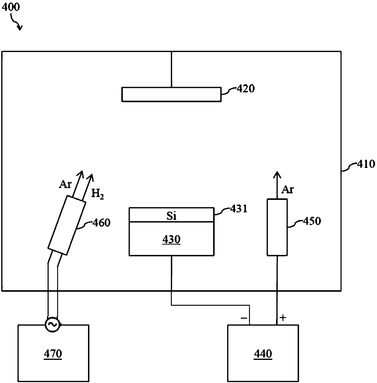
[0055] According to a first aspect of the present invention, a method for preparing a high refractive index hydrogenated silicon film is provided, comprising the following steps:
[0056] (a) Deposit Si on the substrate by magnetron Si target sputtering to form a silicon film;
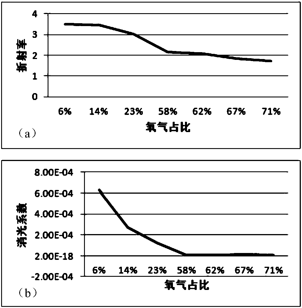
[0057] (b) The silicon film forms an oxygen-containing hydrogenated silicon film in an environment containing active hydrogen and active oxygen, and the amount of active oxygen accounts for 4 to 99% of the total amount of active hydrogen and active oxygen, or,
[0058] The silicon film forms a hydrogenated silicon film containing nitrogen in an environment containing active hydrogen and active nitrogen, and the amount of active nitrogen accounts for 5-20% of the total amount of active hydrogen and active nitrogen.
[0059] In step (a), the Si target is a semiconductor high-purity silicon material in the form of single crystal or polycrystal.
[0060] Typical but non-limiting substrates are, for exampl...
Embodiment 1
[0142] A method for preparing a high-refractive-index hydrogenated silicon film comprising the following steps:
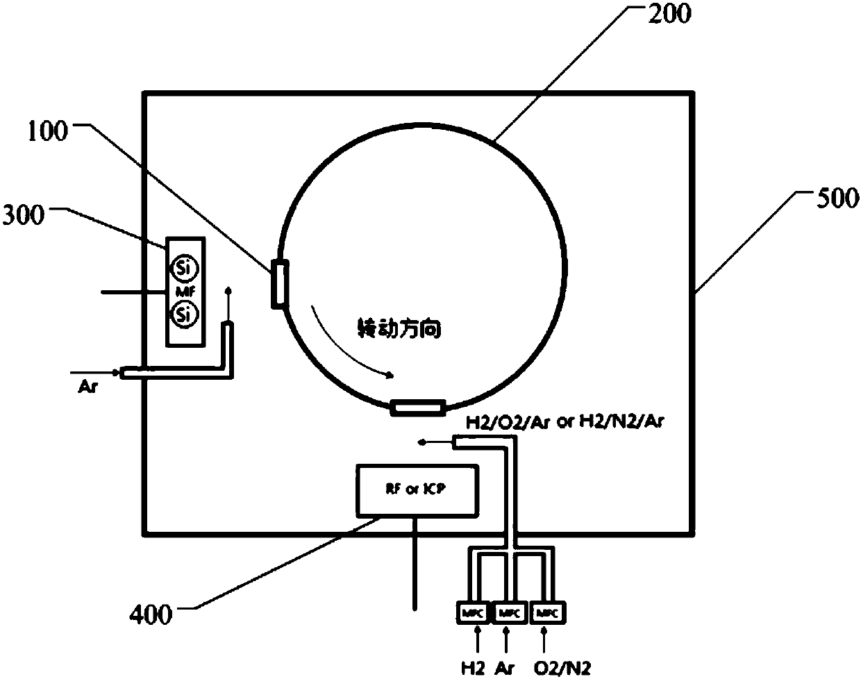
[0143] (a) The clean substrate is placed on the roller with the coated side facing outward;
[0144] (b) The drum rotates at a constant speed in the coating chamber;
[0145] (c) When the vacuum degree is higher than 10 -4 At Pa, turn on the sputtering source and pass argon gas, the power of the sputtering source is 8KW, the argon gas is ionized to form plasma, and bombards the high-purity silicon target under the action of electricity and magnetic field, and the silicon material is sputtered onto the substrate;
[0146] (d) With the rotation of the drum, the substrate is brought to the reaction source area;
[0147] (e) Turn on the reaction source, the power of the reaction source is 2KW, hydrogen, oxygen and argon are fed into the reaction source area, and the gas flow rate is adjusted so that the volume percentage of the incoming oxygen accounted for the sum o...
Embodiment 2
[0149] A method for preparing a high-refractive-index oxygen-containing hydrogenated silicon film. In step (e), the volume percentage of the oxygen fed into the sum of the hydrogen and oxygen fed is 14%, and the rest of the steps and parameters are the same as in Example 1.
PUM
| Property | Measurement | Unit |
|---|---|---|
| thickness | aaaaa | aaaaa |
| thickness | aaaaa | aaaaa |
| thickness | aaaaa | aaaaa |
Abstract
Description
Claims
Application Information


