Silicon nitride-lithium niobate heterogeneous integrated waveguide device structure and preparation method of the same

An integrated waveguide and device structure technology, applied in the direction of optical waveguide light guide, light guide, instrument, etc., can solve the problems of incompatibility of semiconductor processing technology, limitation of large-scale batch production, difficulty of real-time monitoring of polishing process, etc., to achieve compact structure, The effect of compatible processing technology and high extinction ratio

Inactive Publication Date: 2018-03-27
UNIV OF SHANGHAI FOR SCI & TECH
View PDF8 Cites 38 Cited by
  • Summary
  • Abstract
  • Description
  • Claims
  • Application Information

AI Technical Summary

Problems solved by technology

However, the existing integrated technology of chemical mechanical polishing for surface planarization makes silicon nitride materials easy to crack due to changes in film stress, and the polishing process is difficult to monitor in real time, which is incompatible with semiconductor processing technology
Therefore, it is necessary to use the method of secondary photolithography to prepare the stress relief structure, which limits the large-scale mass production
At the same time, domestic integrated optoelectronic devices based on lithium niobate have also been extensively studied, including the growth of lithium niobate thin film materials [Prior Technology 2: Cui Jiao et al., Journal of Synthetic Crystals, 2016,45(5):1266-1270] , device fabrication and related linear and nonlinear optical applications, etc., but not much attention has been paid to the heterogeneous integration of low-loss waveguides and lithium niobate materials. Structural design and implementation of heterogeneous integration of lithium niobate materials on silicon nitride waveguide substrates

Method used


Image

  • Silicon nitride-lithium niobate heterogeneous integrated waveguide device structure and preparation method of the same
  • Silicon nitride-lithium niobate heterogeneous integrated waveguide device structure and preparation method of the same
  • Silicon nitride-lithium niobate heterogeneous integrated waveguide device structure and preparation method of the same

Examples


Embodiment Construction

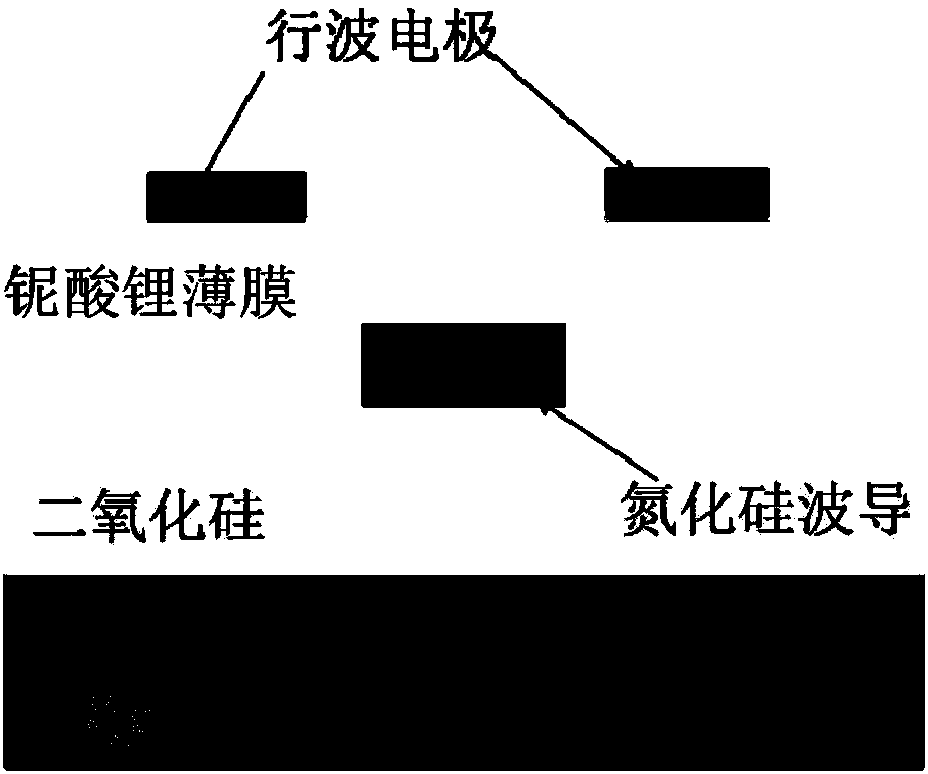
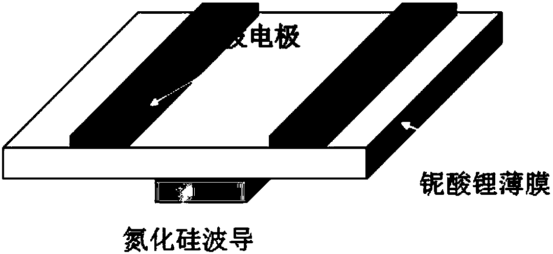
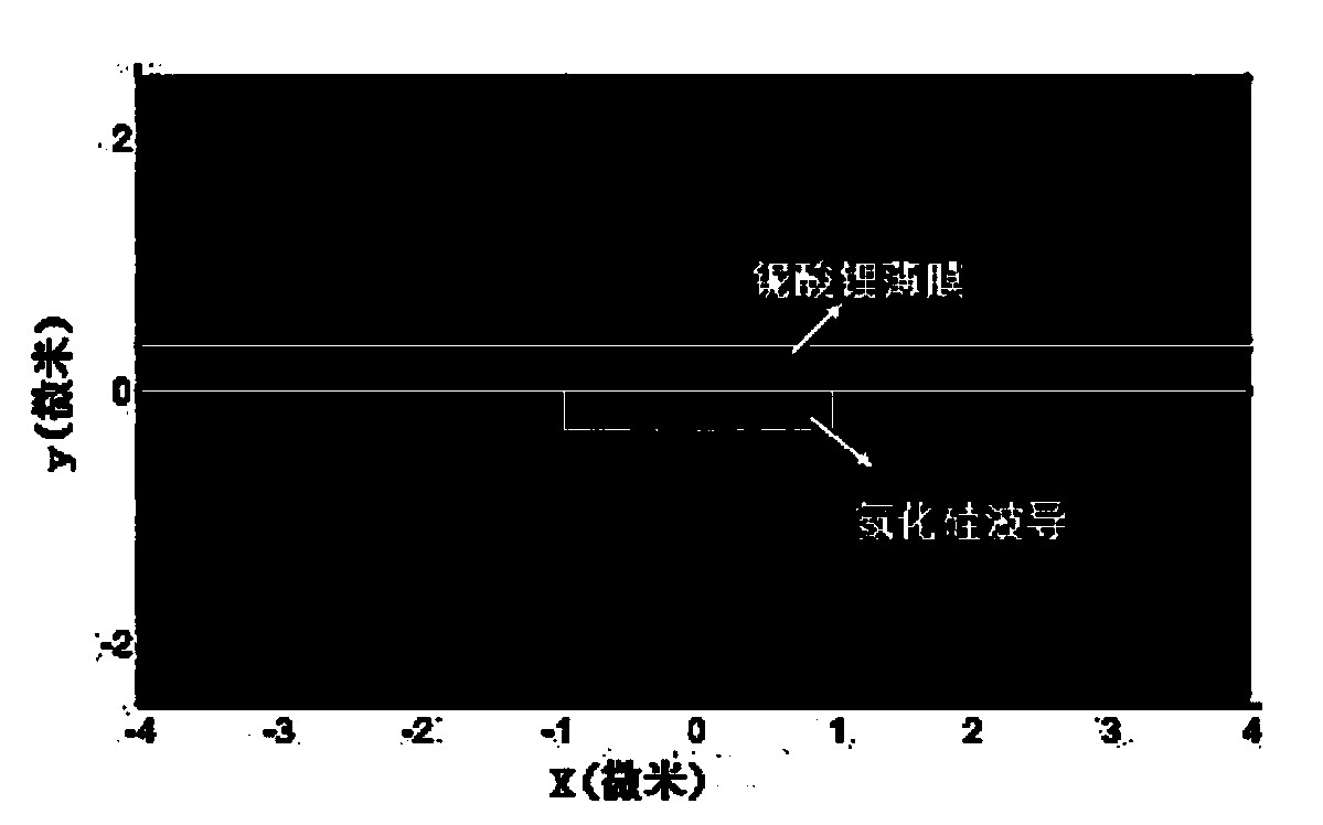
[0023] like figure 1 The cross-sectional view of the silicon nitride waveguide structure of the heterogeneously integrated lithium niobate film is shown. Silicon dioxide is deposited on the surface of the silicon material, and then silicon nitride is deposited and etched to obtain a 350-nanometer thick nitrogen in the silicon dioxide cladding layer. Silicon nitride waveguide, the silicon nitride waveguide is surrounded by silicon dioxide, and then a layer of 400nm thick lithium niobate film is attached. Prepare two traveling wave electrodes on both sides; figure 2 The perspective schematic diagram of the ridge waveguide in the silicon nitride waveguide with heterogeneous integrated lithium niobate thin film shown. like image 3 It describes the mode field diagram simulated by the finite-difference time-domain algorithm of a high-speed optical modulation chip based on heterogeneous integration of silicon nitride and lithium niobate. The upper layer is the modulable content o...


PUM


Abstract

The invention relates to a silicon nitride-lithium niobate heterogeneous integrated waveguide device structure and a preparation method of the same. The silicon nitride-lithium niobate heterogeneous integrated waveguide device structure is characterized in that a silicon nitride waveguide in a silica coating layer and a lithium niobate film on the upper surface of the silicon nitride waveguide areheterogeneously integrated to form a ridge waveguide; a traveling wave electrode is arranged on the upper surface of the lithium niobate film; the silicon nitride waveguide is crossed and coupled with the lithium niobate film on the upper surface of the silicon nitride waveguide, and a high speed electric signal is applied to the traveling wave electrode to control the phase of the light wave passing through the lithium niobate film to realize conversion from amplitude modulation of the loaded electric signal to phase modulation of an optical signal; and three-dimensional vertical integrateddesign is utilized to enable integration of the chip to be more compact, so that the space is saved; at the same time insertion loss of the light waveguide can be reduced; 100G light modulation rate can be realized; high speed modulation of the light wave in the lithium niobate film can be realized and the characteristic of low loss propagation through the silicon nitride waveguide is realized; and light modulation with excellent performance is completed. The manufacturing technology of the silicon nitride-lithium niobate heterogeneous integrated waveguide device structure is compatible with the semiconductor processing technology, is high in the modulation efficiency and low in energy consumption, and has important application prospects in the optical signal processing field and other fields.

Description

technical field [0001] The invention relates to a high-speed optical modulation chip in the optical communication band, in particular to a silicon nitride-lithium niobate heterogeneous integrated waveguide device structure and a preparation method. Background technique [0002] With the advent of the era of big data, the bandwidth and capacity of communication networks are increasing rapidly. Based on the existing traditional optical signal processing devices, not only the bandwidth and speed encounter bottlenecks, but the energy consumed also increases sharply. Therefore, it is urgent to develop ultra-high-speed low-energy new integrated optoelectronic devices. Among them, the optical modulator, as a core device in many fields such as optical information processing, spectral measurement, and optical storage, has developed a variety of devices based on effects such as electro-optic, acousto-optic, and magneto-optical effects. Regulating the amplitude or phase of the output ...

Claims


Application Information

Patent Timeline
Patent Type & Authority Applications(China)
IPC IPC(8): G02B6/12G02B6/13G02B6/136G02F1/035
CPCG02B6/12G02B6/13G02B6/136G02B2006/12038G02B2006/1204G02B2006/12142G02B2006/12176G02F1/035
Inventor 冯吉军翟珊顾昌林霍雨曾和平
Owner UNIV OF SHANGHAI FOR SCI & TECH
Why Eureka
Try Eureka