Preparation method of improved type back surface tunnel oxidization and passivation contact efficient battery

A technology of tunnel oxidation and tunnel oxide layer, which is used in the manufacture of circuits, electrical components, and final products, etc., can solve the problem of not greatly improving electrical performance, improve electrical performance parameters, improve open circuit voltage and conversion efficiency, reduce compound effect

Inactive Publication Date: 2018-03-27
SHANGHAI SHENZHOU NEW ENERGY DEV
View PDF7 Cites 20 Cited by
  • Summary
  • Abstract
  • Description
  • Claims
  • Application Information

AI Technical Summary

Problems solved by technology

[0003] Chinese patent CN102544198A discloses a method for preparing a selective emission crystalline silicon solar cell, including single-step high-concentration doping diffusion, and then printing anti-corrosion paste on the electrode area by printing process, and chemically etching the non-electrode area to achieve light doping The emitter

Method used


Image

  • Preparation method of improved type back surface tunnel oxidization and passivation contact efficient battery

Examples


Embodiment 1

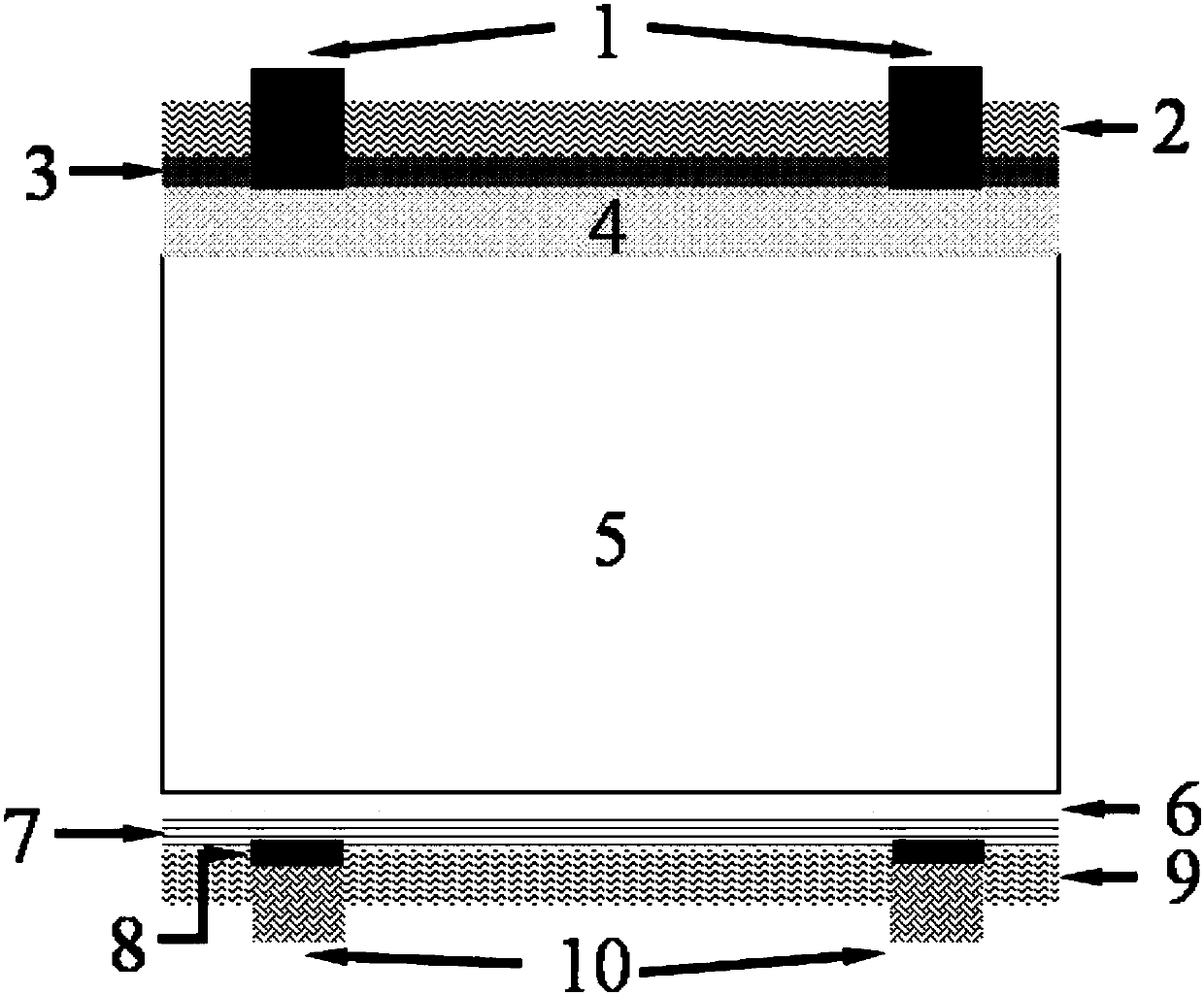
[0030] A method for making a high-efficiency cell with an oxidation passivation contact on the back side of the front emitter junction adopts the following steps:

[0031] (1) Remove the damaged layer of the silicon wafer in KOH alkali solution and make texture, and form a pyramid texture with 1 μm on both sides;

[0032] (2) In the boron source high-temperature diffusion furnace tube, the temperature is controlled at 850°C for 40 minutes to form low surface concentration B-doped p + launch junction;

[0033] (3) Use HF solution to remove borosilicate glass BSG layer, and use HNO 3 Mixed solution with HF for side insulation and back polishing;

[0034] (4) Using wet chemical method to grow an ultra-thin tunnel oxide layer SiO on the back of the silicon wafer 2 , whose thickness is less than 2nm, and then use the PECVD method to grow a P-doped polysilicon layer with a thickness of 20nm on it. This example uses fluorosilicate H 2 SiO 6 solution, the concentration is 1.3M, p...

Embodiment 2

[0041] A method for making a high-efficiency cell with an oxidation passivation contact on the back side of the front emitter junction adopts the following steps:

[0042](1) Remove the damaged layer and texture the silicon wafer in NaOH alkali solution, and form a pyramid texture with 2 μm on both sides;

[0043] (2) In the boron source high-temperature diffusion furnace tube, the temperature is controlled at 900°C for 30 minutes to form low surface concentration B-doped p + launch junction;

[0044] (3) Use HF solution to remove borosilicate glass BSG layer, and use HNO 3 Mixed solution with HF for side insulation and back polishing;

[0045] (4) Using wet chemical method to grow an ultra-thin tunnel oxide layer SiO on the back of the silicon wafer 2 , its thickness is less than 2nm, then use PECVD or other CVD methods to grow a P-doped polysilicon layer with a thickness of 30nm on it, the present embodiment adopts fluorosilicate H 2 SiO 6 solution, the concentration is...

Embodiment 3

[0051] A method for making a high-efficiency cell with an oxidation passivation contact on the back side of the front emitter junction adopts the following steps:

[0052] (1) Remove the damaged layer and texture the silicon wafer in NaOH alkali solution, and form a pyramid texture with 5 μm on both sides;

[0053] (2) In the boron source high-temperature diffusion furnace tube, the temperature is controlled at 1000 ° C for 20 minutes to form low surface concentration B-doped p + launch junction;

[0054] (3) Use HF solution to remove borosilicate glass BSG layer, and use HNO 3 Mixed solution with HF for side insulation and back polishing;

[0055] (4) Using wet chemical method to grow an ultra-thin tunnel oxide layer SiO on the back of the silicon wafer 2 , its thickness is less than 2nm, then use PECVD or other CVD methods to grow a P-doped polysilicon layer with a thickness of 50nm on it, the present embodiment adopts fluorosilicate H 2 SiO 6 Solution, the concentratio...


PUM

PropertyMeasurementUnit
Thicknessaaaaaaaaaa
Thicknessaaaaaaaaaa
Thicknessaaaaaaaaaa

Abstract

The invention relates to a preparation method of an improved type back surface tunnel oxidization and passivation contact efficient battery. The preparation method comprises the steps of performing texturing after a silicon wafer damage layer is removed; next, forming a low surface concentration B doped P<+> emitting junction; after performing edge insulating and back surface polishing, enabling ultra-thin tunnel oxide layer SiO<2> and P-doped polysilicon layer to be grown on the back surface of a silicon wafer; depositing an aluminium oxide layer on the surface of the P<+> emitting junction;enabling a hydrogenated amorphous silicon nitride passivated antireflection layer to be grown on the front surface of the silicon wafer; forming partial heavy doping on the back surface of the siliconwafer by adopting a laser doping or wet etching method; enabling the hydrogenated amorphous silicon nitride passivated antireflection layer to be grown on the back surface of the silicon wafer; and finally, printing Ag/Al paste on the front surface of the silicon wafer, and printing Ag paste on the back surface. By adoption of the layer of the ultra-thin tunnel oxide layer SiO<2>, one layer of phosphorus P-doped silicon layer and the P-doped region partial heavy doping, the metal-semiconductor surface compounding on the back surface can be greatly lowered; and the preparation method has the most obvious advantage of capability of greatly improving electrical performance on the basis of compatibility with the conventional battery manufacturing process.

Description

technical field [0001] The invention relates to a preparation method of a solar cell, in particular to a preparation method of an improved back tunnel oxidation passivation contact high-efficiency cell. Background technique [0002] The difference between the heavily doped tunnel oxidation passivation contact cell technology and the conventional cell technology lies in the preparation of the composite structure of the back tunnel oxidation passivation layer and the doped polysilicon layer, and the back metal contact area uses The key points of this method are the preparation control of the ultra-thin tunnel oxide layer and the treatment of the interface state with the silicon substrate before preparation. [0003] Chinese patent CN102544198A discloses a method for preparing a selective emission crystalline silicon solar cell, including single-step high-concentration doping diffusion, and then printing anti-corrosion paste on the electrode area by printing process, and chemic...

Claims


Application Information

Patent Timeline
IPC IPC(8): H01L31/0224H01L31/0216H01L31/18
CPCH01L31/02167H01L31/022441H01L31/1804H01L31/1868Y02P70/50
Inventor 汪建强吕爱武石磊郑飞林佳继张忠卫阮忠立许卓
Owner SHANGHAI SHENZHOU NEW ENERGY DEV
Why Eureka
Try Eureka