
Method and manufacturing process for removing silicon dioxide from wafer

A technology of silicon dioxide and wafers, which is applied in semiconductor/solid-state device manufacturing, transistors, electrical components, etc., can solve the problems of shrinking isolation layer size, affecting device performance, and low etching selection, so as to reduce substrate damage and reaction The process is simple and the effect of less particles

Pending Publication Date: 2018-04-17
BEIJING NAURA MICROELECTRONICS EQUIP CO LTD
View PDF3 Cites 3 Cited by
  • Summary
  • Abstract
  • Description
  • Claims
  • Application Information

AI Technical Summary

Problems solved by technology

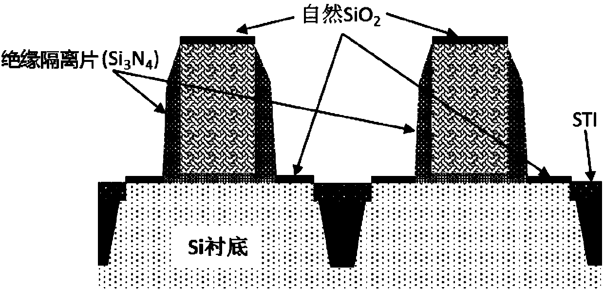
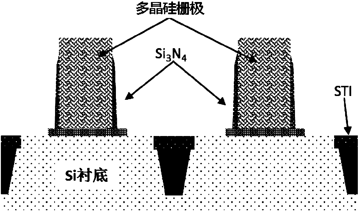
[0003] like Figure 1b As shown, the existing processes mostly use wet etching, plasma dry etching and other methods to remove SiO 2 , for Si 3 N 4 The etching selection ratio is low, and the isolation layer is removed too much, resulting in a reduction in the size of the isolation layer and an increase in leakage, thereby affecting device performance

Method used


Image

  • Method and manufacturing process for removing silicon dioxide from wafer
  • Method and manufacturing process for removing silicon dioxide from wafer
  • Method and manufacturing process for removing silicon dioxide from wafer

Examples


example 1

[0054] Example 1: HARP fill shallow trench insulation layer profile adjustment (STI HAPR deposition gap fill profile modified):

[0055] Figure 4a , 4b and 4c respectively show schematic diagrams of HARP filled shallow trench insulating layer profile adjustment according to the prior art, wherein, Figure 4a For devices after STI (Shallow Trench Isolation) etching, Figure 4b For devices during STI HARP deposition, Figure 4c A device that produces voids after STI HARP deposition; Figure 5a , 5b , 5c and 5d respectively show schematic diagrams of the effect of the method for removing silicon dioxide on the wafer according to the present invention in the process of adjusting the profile of the shallow trench insulating layer filled with HARP, wherein, Figure 5a For devices after STI (Shallow Trench Isolation) etching, Figure 5b For devices during STI HARP deposition, Figure 5c For adopting the method for removing the silicon dioxide on the wafer of the present i...

example 2

[0058] Example 2: STI Si 3 N 4 Natural oxide layer removal:

[0059] Figure 6a and 6b Schematic diagrams of a device with a natural oxide layer and a device after removing the natural oxide layer according to the method of the present invention are respectively shown.

[0060] In this example, the processing steps are the same as Example 1. Such as Figure 6a As shown, the integrated circuit manufacturing process uses Si 3 N 4 As the hard mask (Hard Mask) layer of STI, use H when removing 3 PO 4 Wet removal, after the wafer is placed in the air for a period of time on the Si 3 N 4 The surface of the layer will naturally oxidize a layer of dense SiO 2 layer, while H 3 PO 4 to SiO 2 The removal rate is very slow, so when removing Si 3 N 4 Before removing this layer of natural oxide layer. In addition, the step height of STI (referring to the height of STI above the substrate surface) will affect the electrical performance of the device. This height can neith...

example 3

[0061] Example 3: IC Pad oxide remove:

[0062] Figure 7a and 7b Schematic diagrams of a device with a pad oxide layer and a device after removing the pad oxide layer according to the method of the present invention are respectively shown.

[0063] In this example, the processing steps are the same as Example 1. Such as Figure 7a As shown, the pad oxide layer (Pad oxide) is used as the hard mask layer Si of STI 3 N 4 The buffer layer is thermally oxidized a layer of SiO on the surface of the substrate using a furnace tube method. 2 Layer, the thickness of the 28nm process is about 50A (different thicknesses are selected according to different processes), and it needs to be removed before the subsequent process is manufactured. In addition, STIHARP is SiO deposited by CVD 2 , low density, poor compactness, high etching rate. Etching SiO in prior art 2 The selection ratio of HARP is low, it is not easy to control the step height of STI, and at the same time, a depre...


PUM


Abstract

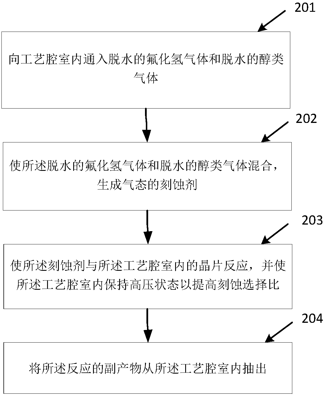
A method and a manufacturing process for removing silicon dioxide from a wafer are disclosed. The method may include the following steps: dehydrated hydrogen fluoride gas and dehydrated alcohol gas are introduced into the process chamber, the dehydrated hydrogen fluoride gas and the dehydrated alcohol gas are mixed to generate a gaseous etchant, the etchant is reacted with the wafer within the process chamber, a high pressure state is maintained in the process chamber to increase an etching selectivity ratio, and byproducts of reaction are withdrawn from the process chamber. According to the method for removing silicon dioxide on the wafer disclosed in the present invention, the gaseous etchant is directly reacted with the silicon dioxide under high pressure, reaction products are extracted after the reaction, and therefore silicon dioxide can be removed with a high selectivity ratio and high efficiency.

Description

technical field [0001] The invention relates to the field of integrated circuit manufacturing technology, and more specifically, relates to a method for removing silicon dioxide on a wafer applied in an integrated circuit manufacturing process and an integrated circuit manufacturing process using the method for removing silicon dioxide on a wafer. Background technique [0002] In the field of integrated circuit manufacturing technology, silicon-based materials are usually used to manufacture integrated circuits. When silicon (or polysilicon) is placed in the air, the surface will naturally oxidize to form a dense layer of silicon dioxide (SiO2). 2 ) layer, such as Figure 1a shown. In some processes, for example, in the metal silicide (Silicide) process, the metal nickel platinum (NiPt) film is in direct contact with the silicon substrate, if there is a layer of SiO on the surface of the substrate 2 , it will increase the resistivity and affect the performance of the device...

Claims


Application Information

Patent Timeline
Patent Type & Authority Applications(China)
IPC IPC(8): H01L21/311H10B41/35
CPCH01L21/31116H01L21/31111H01L21/02057H01L21/02164H01L21/02271H01L21/76224H01L21/76229H10B41/42H01L21/0337H01L21/306H01L21/311H01L29/66825H01L29/788H10B41/35H01L21/67069
Inventor 马振国张军吴鑫
Owner BEIJING NAURA MICROELECTRONICS EQUIP CO LTD
Learn More