CdTe thin film solar battery taking SnTe as back electrode buffer layer, and preparation method of thin film solar battery
A technology of solar cells and buffer layers, applied in circuits, photovoltaic power generation, electrical components, etc., can solve problems such as low carriers, limiting the increase of battery open circuit voltage, and limiting conversion efficiency.
- Summary
- Abstract
- Description
- Claims
- Application Information
AI Technical Summary
Problems solved by technology
Method used
Image
Examples
Embodiment 1
[0061] Embodiment 1: CdTe thin-film solar cell of single-layer SnTe buffer layer 5
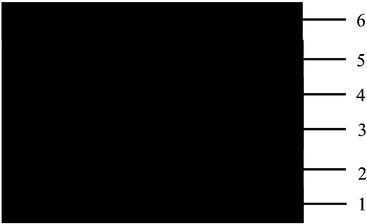
[0062] use figure 1 battery structure.
[0063] Transparent conductive glass layer 1: The conductive glass is purchased directly, and has a fluorine-doped tin oxide conductive layer of about 600nm on it. The conductive glass is cleaned with glass cleaner, absolute ethanol and pure water in sequence, and then blown dry with nitrogen.
[0064] Preparation of high resistance layer 2 and window layer 3: using magnetron sputtering method, in a low vacuum environment, continuously deposit 20nm Zn 2 SnO 4 And 60nm CdS film.
[0065] The preparation of the absorbing layer 4: the close-distance sublimation method is adopted, the temperature of the substrate is controlled at 600° C., the temperature of the CdTe evaporation source is controlled at 650° C., and nitrogen gas is introduced as a protective gas. The thickness of the deposited CdTe film is about 4 microns.
[0066] CdCl for absorber laye...
Embodiment 2
[0070] Embodiment 2: ZnTe: CdTe thin film solar cell of Cu / SnTe buffer layer 5
[0071] use figure 1 battery structure.
[0072] Transparent conductive layer: The conductive glass is purchased directly, with a fluorine-doped tin oxide conductive layer of about 600nm on it. The conductive glass is cleaned with glass cleaner, absolute ethanol and pure water in sequence, and then blown dry with nitrogen.
[0073] Preparation of high resistance layer 2 and window layer 3: using magnetron sputtering method, in a low vacuum environment, continuously deposit 20nm Zn 2 SnO 4 And 60nm CdS film.
[0074] The preparation of the absorbing layer 4: the close-distance sublimation method is adopted, the temperature of the substrate is controlled at 600° C., the temperature of the CdTe evaporation source is controlled at 650° C., and nitrogen gas is introduced as a protective gas. The thickness of the deposited CdTe film is about 4 microns.
[0075] CdCl for absorber layer 4 2 Treatmen...
PUM
 Abstract
Description
Claims
Application Information


