

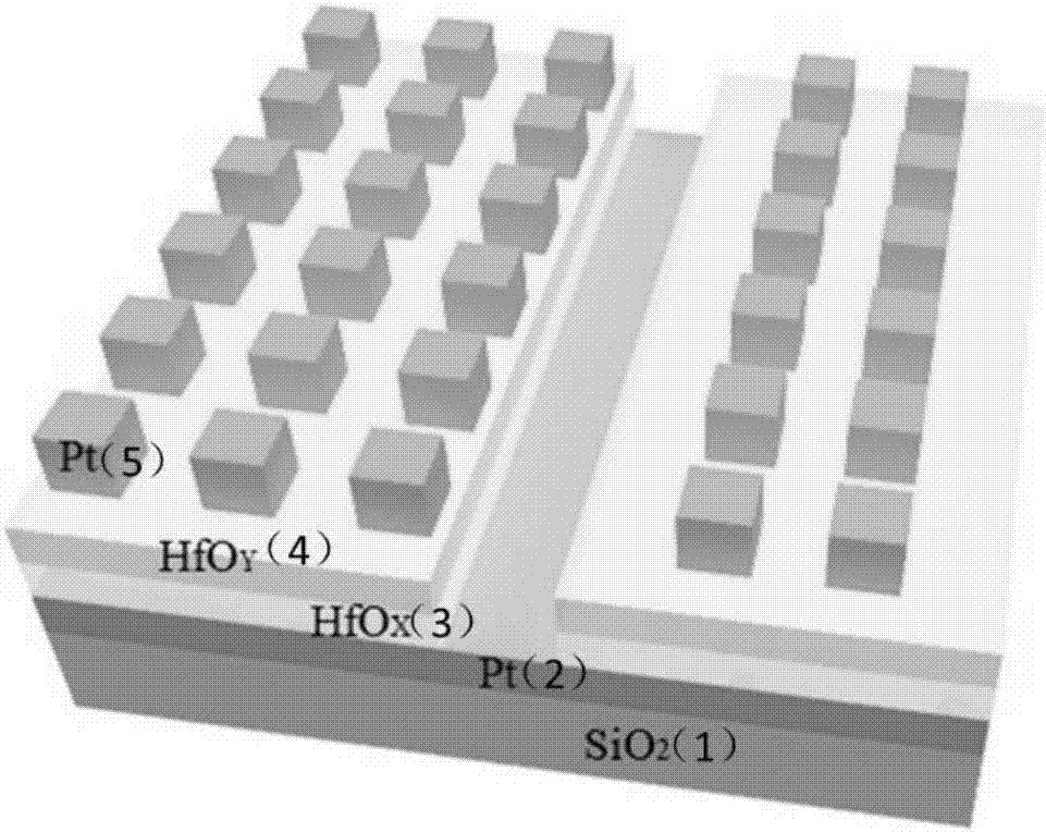
Laminated HfO2-based resistive random access memory for improving current overcharging, and manufacturing method thereof
A technology of resistive variable memory and manufacturing method, which is applied in the field of microelectronics, can solve problems such as inability to reduce switching voltage, high switching voltage, large overshoot current, etc., achieves improvement of current overshoot phenomenon, improvement of device performance, and simple structure Effect
- Summary
- Abstract
- Description
- Claims
- Application Information
AI Technical Summary
Problems solved by technology
Method used
Image

Examples
Embodiment 1
[0031] Embodiment 1, making HfO x The oxygen-argon ratio of the oxygen supply layer is 15% and HfO y The resistive switch layer has an oxygen-argon ratio of 40% laminated HfO 2 Base RRAM.
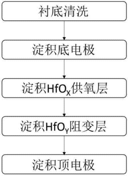
[0032] Step 1, cleaning SiO2 2 substrate.
[0033] First clean the substrate silicon wafer with acetone ultrasonically for 3 minutes, and the ultrasonic intensity is 3.0;
[0034] Then ultrasonically clean the substrate silicon wafer with ethanol for 2 minutes, and the ultrasonic intensity is 3.0;
[0035] Then rinse the substrate silicon wafer with ultrapure water for 2 minutes, then take out the silicon wafer and dry it with nitrogen;
[0036] Finally, the surface of all substrate silicon wafers is inspected with a microscope to ensure that the surface is clean.
[0037] Step 2, depositing the bottom electrode.
[0038] Using PVD DC sputtering process, the cleaned SiO 2 Deposit a metal Pt bottom electrode with a thickness of 115nm on the silicon wafer:
[0039] PVD DC sputtering ...
Embodiment 2
[0072] Embodiment 2, making HfO x The oxygen-argon ratio of the oxygen supply layer is 18% and HfO y The resistive switch layer has an oxygen-argon ratio of 43% laminated HfO 2 Base RRAM.
[0073] Step 1, cleaning SiO2 2 substrate.
[0074] The specific implementation of this step is the same as step 1 of Embodiment 1.
[0075] Step 2, depositing the bottom electrode.
[0076] Using PVD DC sputtering at a vacuum of 5e -6 Torr, the sputtering power is 100W, the argon pressure is 4mTorr, the pre-sputtering time is 180s, and the sputtering time is 750s, the cleaned SiO 2 A metal Pt bottom electrode with a thickness of 120 nm is deposited on the silicon wafer.
[0077] Step 3, Deposit HfO x Support layer.
[0078] Using PVD reactive sputtering at a vacuum of 5e -6 Torr, the sputtering power is 100W, the pulse frequency is 100Hz, the pulse width is 2μs, the gas pressure is 4mTorr, the oxygen-argon ratio is 18%, and the sputtering time is 700s. 18% HfO with argon ratio x...
Embodiment 3
[0083] Embodiment 3, making HfO x The oxygen-argon ratio of the oxygen supply layer is 20% and HfO y Resistive layer with oxygen-argon ratio of 45% laminated HfO 2 Base RRAM.
[0084] Step 1, cleaning the Si wafer substrate.
[0085] The specific implementation of this step is the same as step 1 of Embodiment 1.
[0086] Step 2, depositing the bottom electrode.
[0087] Using PVD DC sputtering at a vacuum of 5e -6 Torr, the sputtering power is 100W, the argon pressure is 4mTorr, the pre-sputtering time is 180s, and the sputtering time is 780s, a layer of metal Pt substrate with a thickness of 125nm is deposited on the cleaned Si silicon wafer. electrode.
[0088] Step 3, Deposit HfO x Support layer.
[0089] Using PVD reactive sputtering at a vacuum of 5e -6 Torr, the sputtering power is 100W, the pulse frequency is 100Hz, the pulse width is 2μs, the gas pressure is 4mTorr, the oxygen-argon ratio is 18%, and the sputtering time is 800s. 20% HfO with argon ratio x Su...
PUM
 Abstract
Description
Claims
Application Information