A gold nanoring stacked array substrate with surface-enhanced Raman scattering and its preparation method

A surface-enhanced Raman and array substrate technology, which is used in Raman scattering, photolithography on patterned surfaces, opto-mechanical equipment, etc., can solve the problem of not being able to meet the requirements of large area, uniformity and high enhanced signal of SERS substrates at the same time. , it is difficult to control the particle spacing and other problems, to achieve the effect of easy large-area preparation, strong Raman signal enhancement effect, and easy control of the period

Active Publication Date: 2020-05-15
CHANGCHUN UNIV OF SCI & TECH
View PDF7 Cites 0 Cited by
  • Summary
  • Abstract
  • Description
  • Claims
  • Application Information

AI Technical Summary

Problems solved by technology

By synthesizing a wide variety of templates, plasmonic nanostructures can also take various forms, but so far, it is difficult to control the particle distance due to the limitations of the method.
[0007] In summary, none of the above methods can meet the requirements of large area, uniformity and high enhanced signal of SERS substrate at the same time.

Method used


Image

  • A gold nanoring stacked array substrate with surface-enhanced Raman scattering and its preparation method
  • A gold nanoring stacked array substrate with surface-enhanced Raman scattering and its preparation method
  • A gold nanoring stacked array substrate with surface-enhanced Raman scattering and its preparation method

Examples


Embodiment 1

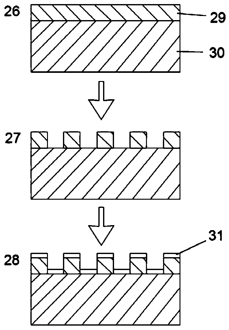
[0041] (1) cleaning the substrate, with a thickness of 1.2 mm single-sided polished silicon as the substrate material 30, its reflectivity in the visible light range is higher than 80%, it is placed in acetone, absolute ethanol, deionized water for ultrasonic cleaning, Blow dry with high-purity nitrogen for 100-150s each time, select positive photoresist 29, the type is AR-P3740 for glue coating, the resolution is 0.5μm, the rotation speed of the homogenizer is 4000r / min, and the thickness of the glue is 1.5μm, then put it on a hot plate, pre-baked at 100°C, the pre-baked time is 1min, take it off, and place it in dark conditions, such as image 3 The gluing process in is shown in 26;

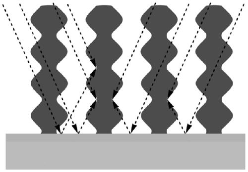
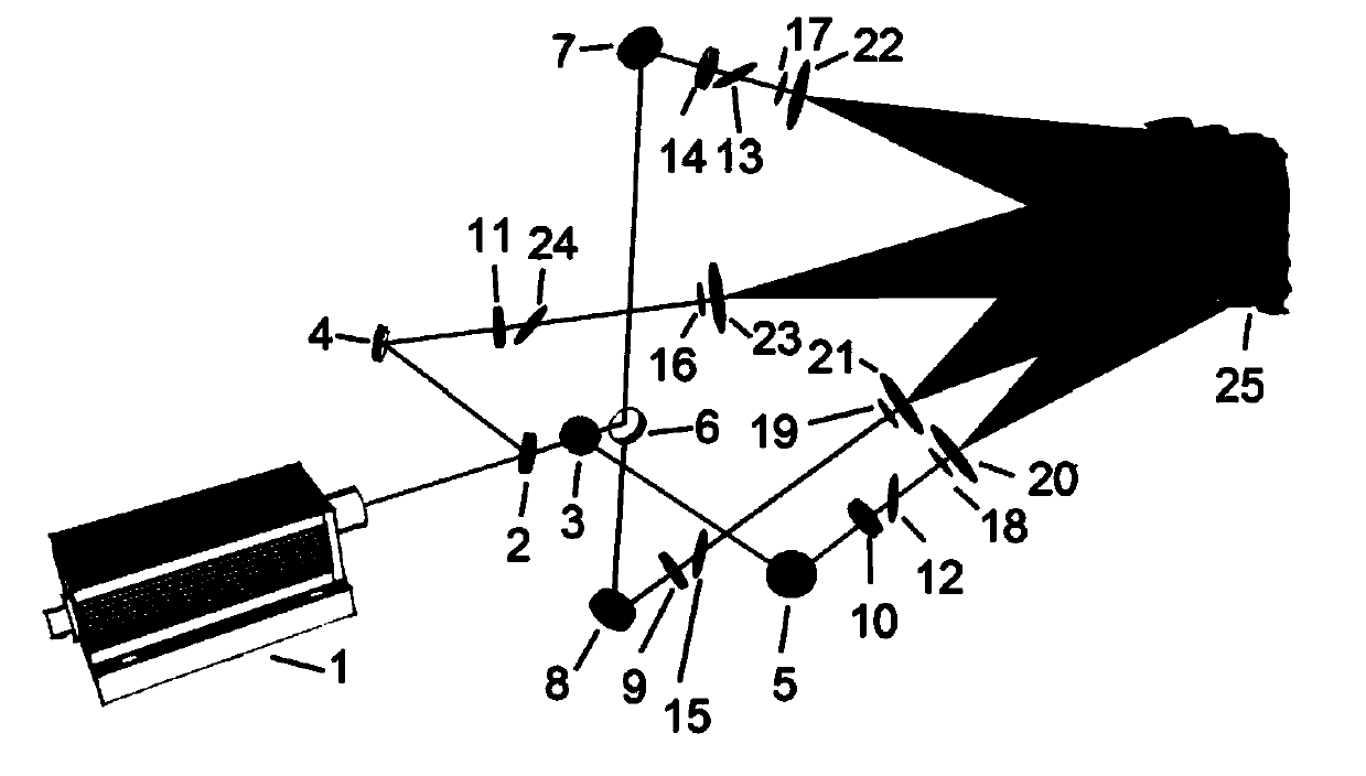
[0042] (2) Exposure is performed using a four-beam laser interference lithography system. The four-beam interference system generates modulation by controlling the incident angle. A 360nm semiconductor laser is the light source for the system, such as figure 2 As shown, the beam emitted by th...

Embodiment 2

[0047] (1) cleaning the substrate, with a thickness of 1.2 mm single-sided polished silicon as the substrate material 30, its reflectivity in the visible light range is higher than 80%, it is placed in acetone, absolute ethanol, deionized water for ultrasonic cleaning, Blow dry with high-purity nitrogen for 100-150s each time, select positive photoresist 29, the type is AR-P3740 for glue coating, the resolution is 0.5μm, the rotation speed of the homogenizer is 4000r / min, and the thickness of the glue is 1.5μm, then put it on a hot plate, pre-baked at 100°C, the pre-baked time is 1min, take it off, and place it in dark conditions, such as image 3 The gluing process in is shown in 26;

[0048] (2) Use a non-modulating three-beam interference lithography system for exposure. The incident angles of the first beam and the second beam of coherent light in the three beams are both 14°. At the same time, the spatial angles of the first beam of coherent light are respectively is 0°,...


PUM

PropertyMeasurementUnit
thicknessaaaaaaaaaa
diameteraaaaaaaaaa
thicknessaaaaaaaaaa

Abstract

The invention discloses a gold nano-ring stacked array substrate with surface-enhanced Raman scattering and a preparation method. The standing wave effect in the photolithography process is utilized, that is, the surface reflection of the incident light substrate material interferes with the incident light, and the photoresist At the same time, the multi-beam laser interference lithography technology arranges the stacked three-dimensional structure according to the specified periodic distribution, and then sputters a nanometer-thick gold film to form a gold nanoring stack. The structure has the effect of surface-enhanced Raman scattering, and can be used as a base material for Raman scattering detection, thereby effectively improving the Raman signal of the detected substance.

Description

technical field [0001] The invention relates to a gold nano ring stacked array substrate with surface-enhanced Raman scattering and a preparation method, belonging to the field of nano material processing. Background technique [0002] Compared with other spectroscopic techniques, Raman spectroscopy has unique advantages, which are mainly reflected in the following aspects: (1) Raman spectroscopy detects the change of light frequency, which is not directly related to the wavelength of the excitation light source, so it can be tested according to the The characteristics of the material, fluorescence characteristics, etc. select the appropriate excitation light wavelength; (2) Raman spectrum is not affected by water, especially suitable for non-destructive testing and on-line testing of samples in the biological field; (3) Raman spectrum detection is not strict on samples Requirements, no sample preparation is required, and usually only a small amount of sample is required to ...

Claims


Application Information

Patent Timeline
Patent Type & Authority Patents(China)
IPC IPC(8): G01N21/65G03F7/20
CPCG01N21/658G03F7/2053
Inventor 董莉彤王作斌张子昂王璐李理周东杨刘梦楠翁占坤宋正勋许红梅
Owner CHANGCHUN UNIV OF SCI & TECH
Why Eureka
Try Eureka