MEMS optical device, light absorption nano structure and preparation method thereof

A nanostructure and light absorption technology, applied in optical components, optics, nanotechnology, etc., can solve the problems of relying on control process accuracy, application field limitations, and high preparation costs, achieving simple and convenient process, low processing cost, and improved absorption capacity. Effect

Pending Publication Date: 2018-05-04
INST OF MICROELECTRONICS CHINESE ACAD OF SCI
View PDF7 Cites 23 Cited by
  • Summary
  • Abstract
  • Description
  • Claims
  • Application Information

AI Technical Summary

Problems solved by technology

However, the multi-layer alternating structure requires alternate deposition of metal layers and dielectric layers, which is difficult in process and high in preparation cost.
Although the method of changing the surface metal morphology of the sandwich structure can control the plasmon action band of the surface metal nanostructure, and the superposition of absorption peaks can broaden the wavelength range of light absorption, but this will introduce the need to control the surface metal morphology. The special process makes this type of structure very dependent on the precision of the control process, and its application fields will also be limited

Method used


Image

  • MEMS optical device, light absorption nano structure and preparation method thereof
  • MEMS optical device, light absorption nano structure and preparation method thereof
  • MEMS optical device, light absorption nano structure and preparation method thereof

Examples


preparation example Construction

[0051] The preparation method of the disclosed light-absorbing nanostructure comprises the following steps:

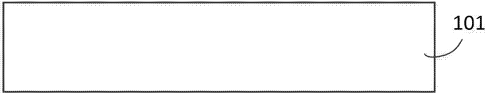
[0052] provide the basis;

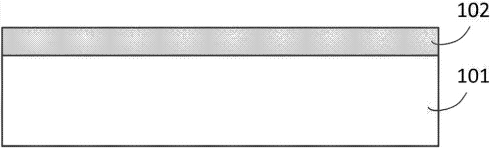
[0053] forming a polymer layer on the substrate;

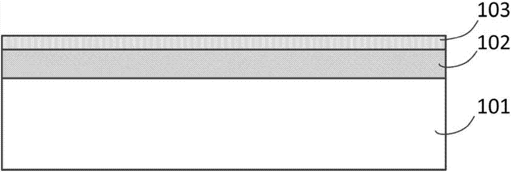
[0054] forming a nanoforest structure using the polymer layer; and

[0055] The nano-forest structure is covered with metal nanoparticles and / or metal nano-films.

[0056] Further, the preparation method of the light-absorbing nanostructure may further include: sequentially forming a specular metal reflection layer and a planar dielectric layer between the substrate and the polymer layer, and further, between the planar dielectric layer and the polymer layer A silicon thin film layer may be formed.

[0057] Furthermore, the preparation method of the light-absorbing nanostructure may further include: forming a titanium nitride adhesion layer between the specular metal reflection layer and the substrate.

[0058] Specifically, the different nano-forest structures are formed by using plasma...

Embodiment 1

[0068] In this embodiment, single crystal silicon is used as the substrate, and an aluminum mirror metal reflective layer and a silicon oxide planar dielectric layer are sequentially formed on the substrate by a sputtering process and a plasma-enhanced chemical vapor deposition (PEVCD) process, thus forming a multilayer optical Reflective and optically coupled substrates. The nanofiber forest structure is formed by sequentially bombarding the polyimide positive photoresist layer with oxygen and argon plasma, and the metal nanostructure is silver nanoparticles or silver nanofilms formed by sputtering metallic silver on the nanofiber forest structure . The method is realized based on conventional micro-nano processing technology, the preparation process is simple and convenient, and large-scale commercial production can be realized.

[0069] refer to Figures 1 to 7 , the preparation method of the light-absorbing nanostructure according to Embodiment 1 of the present disclosur...

Embodiment 2

[0090] In this embodiment, a silicon film layer is formed on a multi-layer light reflection and light coupling substrate, and a nanofiber forest structure is further formed on the silicon film layer, and a nanocone is formed by anisotropic etching using the nanofiber forest structure as a mask The nanofiber has a double-layer forest structure, and through subsequent metal sputtering, a metal nanofilm is formed on the upper nanofiber, and metal nanoparticles are formed on the lower nanocone, finally forming a double-layer light-absorbing nanostructure.

[0091] Please refer to Figures 8 to 12 , the preparation method of the light-absorbing nanostructure in Example 2 of the present disclosure specifically includes the following steps:

[0092] S21, providing a multilayer light reflection and light coupling substrate.

[0093] The multilayer light reflecting and light coupling substrate comprises Figure 8 Shown are a second substrate 201 , a specular metal reflection layer 20...


PUM

PropertyMeasurementUnit
thicknessaaaaaaaaaa
thicknessaaaaaaaaaa
thicknessaaaaaaaaaa

Abstract

The invention provides an MEMS optical device, a light absorption nano structure and a preparation method thereof. The preparation method of the light absorption nano structure comprises the followingsteps of providing a substrate; forming a polymer layer on the substrate; forming a nano forest structure by utilizing the polymer layer; and covering metal nano-particles or a metal nano-film on thenano forest structure. The method disclosed by the invention combines the light trapping effect of the nano forest structure and the surface plasmon effect of the metal nano structure, so that the wide-spectrum high-absorption function is achieved.

Description

technical field [0001] The invention relates to a MEMS optical device, a light-absorbing nanostructure and a preparation method thereof, in particular to a wide-spectrum high-absorption MEMS optical device, a light-absorbing nanostructure and a preparation method thereof. Background technique [0002] Light-absorbing nanostructures are an important part of MEMS optical devices, which directly affect the working performance, manufacturing cost and application range of the devices. The wide-spectrum high-absorption nanostructure can efficiently and indiscriminately absorb the incident light acting on the device, thereby greatly improving the working efficiency of the device. [0003] At present, a variety of broad-spectrum high-absorption nanostructures and their preparation methods have been studied, including black silicon nanostructures, gold-black nanostructures, and surface plasmon nanostructures. However, existing light-absorbing nanostructures still have many defects. ...

Claims


Application Information

Patent Timeline
Patent Type & Authority Applications(China)
IPC IPC(8): G02B26/08B82Y20/00B82Y40/00
CPCB82Y20/00B82Y40/00G02B26/08G02B26/0816
Inventor 杨宇东毛海央
Owner INST OF MICROELECTRONICS CHINESE ACAD OF SCI
Why Eureka
Try Eureka