A method for growing lead zirconate titanate (pzt) nanorings using pulsed laser deposition

A technology of pulsed laser deposition and lead zirconate titanate, which is applied in the direction of nanotechnology, nanotechnology, nanotechnology, etc. for materials and surface science, can solve the problem of inability to prepare miniaturized and portable ferroelectric memory, PZT micro-nano The structure cannot realize precise control and does not conform to the development trend of the information society, etc., to achieve the effect of fast reading speed, low equipment requirements and good reproducibility

Active Publication Date: 2019-10-25
HARBIN INST OF TECH SHENZHEN GRADUATE SCHOOL
View PDF2 Cites 0 Cited by
  • Summary
  • Abstract
  • Description
  • Claims
  • Application Information

AI Technical Summary

Problems solved by technology

However, this method is difficult to process, and the PZT micro-nano structure cannot be precisely regulated, and the PZT thick film is used as the ferroelectric layer of the memory, and it is impossible to prepare a miniaturized and portable ferroelectric memory, which does not conform to the development trend of the information society.

Method used


Image

  • A method for growing lead zirconate titanate (pzt) nanorings using pulsed laser deposition
  • A method for growing lead zirconate titanate (pzt) nanorings using pulsed laser deposition
  • A method for growing lead zirconate titanate (pzt) nanorings using pulsed laser deposition

Examples


Embodiment 1

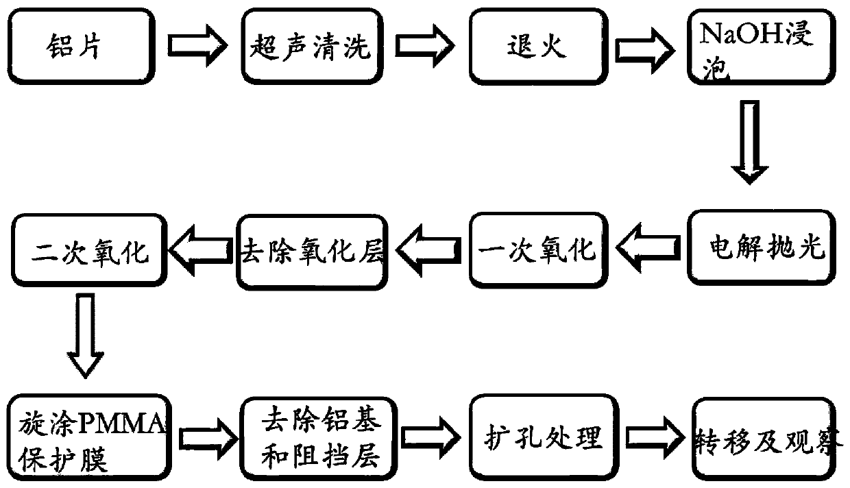
[0038] The whole technical solution is divided into the following five steps:

[0039] Step (1): Select the laser and target;

[0040] Step (2): preparing an AAO template;

[0041] Step (3): cleaning the substrate and transferring the AAO template;

[0042] Step (4): Depositing PZT by PLD method;

[0043] Step (5): removing the AAO film.

[0044] Below are detailed instructions for each step.

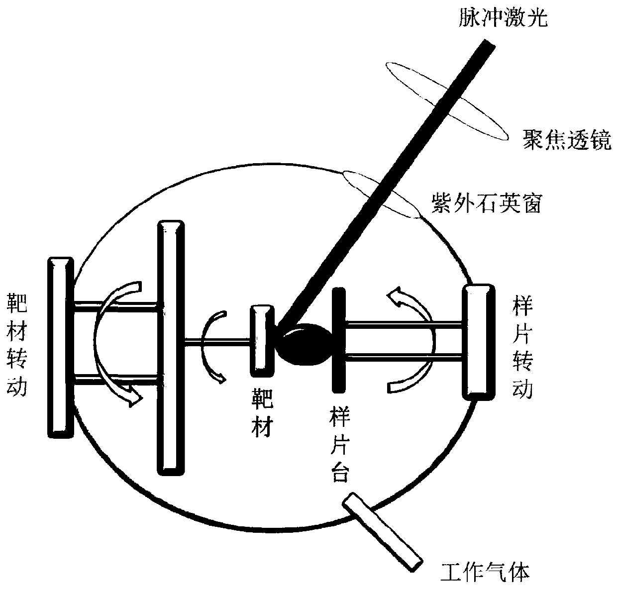
[0045] In the step (1), the laser is a KrF excimer laser with a wavelength of 248nm, and the target is a PZT target with a purity of 99.9%.

[0046] In the step (2), an ultra-thin AAO film is prepared using a two-step anodic oxidation method, figure 1 Shown is a schematic diagram of the preparation process, and the specific process is:

[0047] (a) Pretreatment: the purity is 99.99% aluminum foil, cut into 2cm*2cm. Ultrasonic treatment in acetone, isopropanol, ethanol, and deionized water for 15 minutes, then annealing at 500°C for 3 hours, and then placing in 1mol / L NaOH solution ...

Embodiment 2

[0058] This example provides a PZT nanoring prepared under another experimental parameter. The difference from Example 1 is:

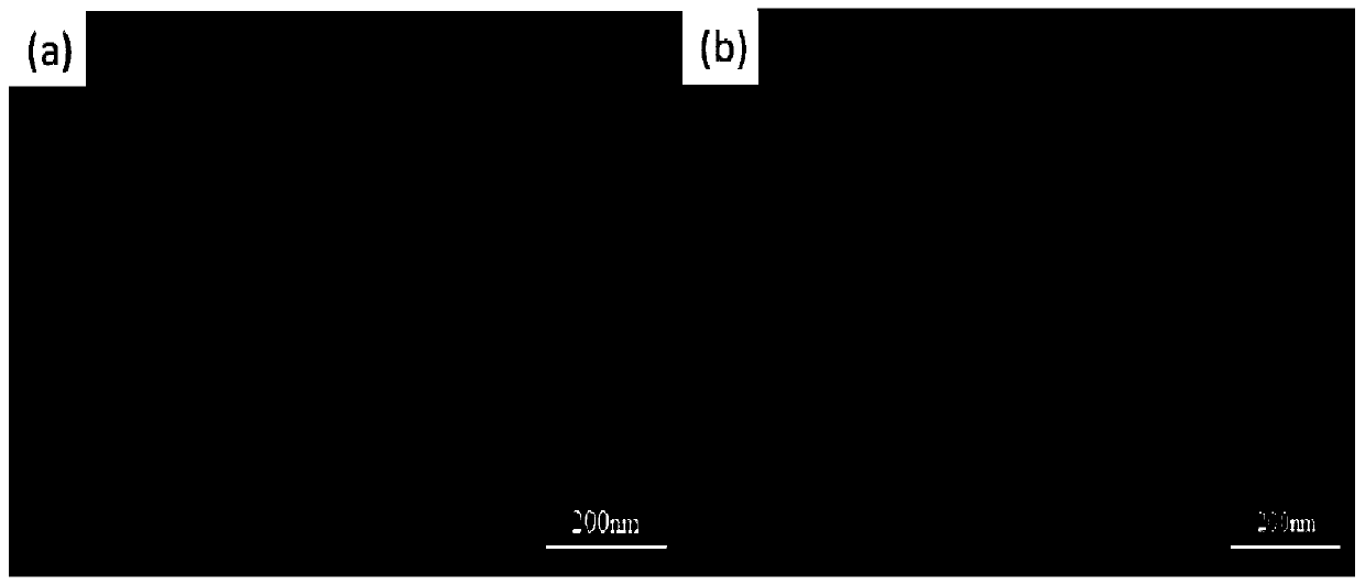
[0059] In the step (4), the sample stage was raised to 550° C., and kept at an annealing temperature of 750° C. for 30 minutes, and the rest of the experimental conditions were kept the same. Image 6 The PZT nanorings prepared under this condition were found to be less regular than the PZT nanorings in Example 1. The diameter of the PZT nanorings was about 80nm, and the wall thickness was about 21nm.

Embodiment 3

[0061] This example provides the substrate as Si / SiO 2 Structured PZT nanorings prepared under silica wafers. The difference from Example 1 is:

[0062] In described step (3), select Si / SiO 2 Structured silicon dioxide wafers were ultrasonically cleaned with acetone, isopropanol, ethanol, and deionized water for 10 min, and then washed with N 2 Blow dry and perform ozone cleaning for 15 minutes.

[0063] In the step (4), the sample stage was raised to 550° C., and kept at an annealing temperature of 750° C. for 30 minutes, the oxygen pressure was adjusted to 25 Pa, and the rest of the experimental conditions were kept the same. Figure 7 It is the XRD pattern of the PZT nanoring prepared under this condition. It can be seen that the PZT diffraction peak is stronger near 31°, corresponding to the (110) crystal plane, which is a perovskite structure. Figure 8 It is the SEM image of the prepared PZT nano-rings, the PZT nano-rings are arranged regularly and have good order. ...


PUM

PropertyMeasurementUnit
wavelengthaaaaaaaaaa
diameteraaaaaaaaaa

Abstract

The invention discloses a method for growing lead zirconate titanate (PZT) nanorings by using the pulsed laser deposition (PLD) technology. The PLD method is used, and preparation of the PZT nanoringsis realized by precisely controlling the deposition temperature, the annealing temperature, annealing time, the number of laser pulses, oxygen pressure and other parameters. The method can be used for preparing regularly arrayed PZT nanorings, parameter control is simple and convenient, repeatability is high, and no toxic and harmful exhaust gas is emitted. The method provides a possibility for the application of high-density ferroelectric memory devices in the future.

Description

technical field [0001] The invention relates to a technology for growing lead zirconate titanate (PZT) nano rings by using pulsed laser deposition technology. Background technique [0002] Low-dimensional nanomaterials (such as nanodots, nanorings, and nanowires) exhibit many exotic optical, electrical, and magnetic properties due to their quantum size effects and quantum confinement effects. Storage and other fields have broad application prospects. As a ferroelectric material with excellent performance, lead zirconate titanate has a high Curie point, good ferroelectric and piezoelectric properties, and will be widely used in the field of high-density ferroelectric storage in the future. But for the preparation of low-dimensional nano-arrays, the traditional photolithography technology can no longer meet the requirements. Therefore, a new and effective way to replace the traditional photolithography technology is urgently needed. [0003] In recent years, a template synth...

Claims


Application Information

Patent Timeline
Patent Type & Authority Patents(China)
IPC IPC(8): C23C14/02C23C14/08C23C14/34C25D11/10C25D11/12C25D11/16C23C28/04B82Y30/00B82Y40/00
CPCB82Y30/00B82Y40/00C23C14/024C23C14/088C23C14/3485C23C28/04C25D11/10C25D11/12C25D11/16
Inventor 刘向力王斌
Owner HARBIN INST OF TECH SHENZHEN GRADUATE SCHOOL
Why Eureka
Try Eureka