Method for preparing non-layered two-dimensional nano-cadmium sulfide crystal material and product
A two-dimensional nano and crystalline material technology, applied in the growth of polycrystalline materials, chemical instruments and methods, nanotechnology, etc., can solve the problems of difficult transfer device processing, weak interlayer force, complex process, etc., and achieve cadmium and sulfur Uniform distribution of elements, increase the reaction energy barrier of the crystal surface, and the effect of smoothing the surface of the crystal surface
- Summary
- Abstract
- Description
- Claims
- Application Information
AI Technical Summary
Problems solved by technology
Method used
Image

Examples
preparation example Construction
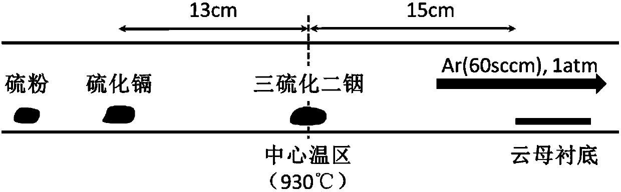
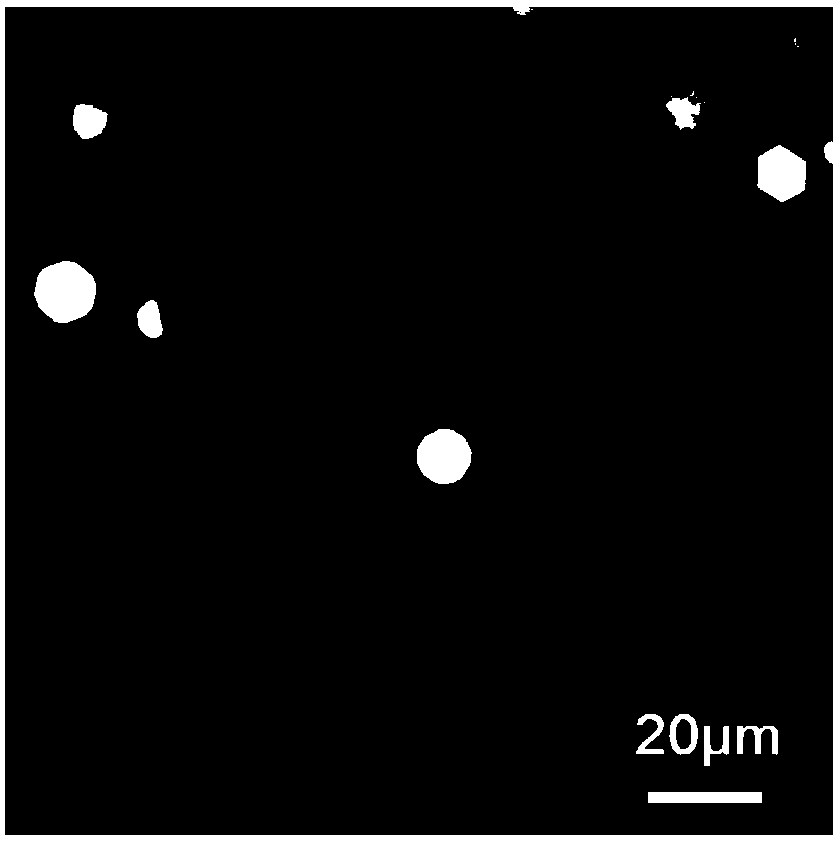
[0030] figure 1 It is a schematic diagram of the preparation of the non-layered two-dimensional nano-cadmium sulfide crystal material constructed according to the preferred embodiment of the present invention, such as figure 1 As shown, the present invention provides a method for preparing a two-dimensional non-layered nano-CdS crystal material (the thickness of a single crystal is below 10 nanometers), thereby producing a large number of two-dimensional CdS crystals with smooth surface, large size, ultrathin, and uniform element distribution material, the compound can be used to manufacture micro-nano optoelectronic devices, etc. The preparation method includes:
[0031] (1) Using a tube furnace, the preparation temperature ranges from 870°C to 950°C;
[0032] (2) Select Cd source and S source and place them in the upstream area, which is 13-18 cm away from the central area. The Cd source is cadmium sulfide or cadmium chloride, and the S source is elemental sulfur;
[0033...
Embodiment 1
[0039] Example of elemental sulfur and cadmium sulfide as reaction source substances and diindium trisulfide as surface inhibitor
[0040] A horizontal tube furnace is adopted, the tube length is 80cm, the range of the constant temperature zone is ±10cm, the temperature in the central area is set to 930°C, the heating rate is 30°C / min, and 10mg of diindium trisulfide is placed in the central area;
[0041] Select cadmium sulfide (CdS) (>98%) 5mg as the cadmium source and sulfur source, select sulfur powder (S) 20mg (≥99%) as the supplementary sulfur source, and these two substances are placed close to each other independently (not mixed) respectively Place a distance of 13 cm from the central area and 18 cm upstream. Directly adopt commercially available mica as the substrate, and place it in the downstream area at a distance of 15 cm from the central area to receive the product;
[0042] Before the reaction, pre-evacuate to about 10Pa atmospheric pressure, then fill it with ...
example 2
[0044] A horizontal tube furnace is used, with a tube length of 80cm, a constant temperature zone range of ±10cm, the temperature in the central area is set to 870°C, the heating rate is 30°C / min, and 15mg of indium chloride is placed in the central area;
[0045] Choose cadmium chloride (Cdcl) (>98%) 8mg as cadmium source and sulfur source, choose sulfur powder (S) 30mg (≥99%) as supplementary sulfur source, and these two substances are placed independently close to each other (not mixed) Place the distances at the upstream area of 13cm and 21cm from the central area, respectively. Directly adopt commercially available mica as the substrate, and place it in the downstream area at a distance of 18 cm from the central area to receive the product;
[0046] Before the reaction, pre-evacuate to about 10Pa atmospheric pressure, then fill it with Ar to atmospheric pressure, and repeat gas washing for at least 3 times to eliminate residual oxygen. During the reaction, Ar (150 sccm...
PUM
| Property | Measurement | Unit |
|---|---|---|
| Thickness | aaaaa | aaaaa |
Abstract
Description
Claims
Application Information