Method for preparing nonenzymatic biosensor based on microelectrode array

A technology of microelectrode array and biosensor, which is applied in the field of photolithography and electrochemical sensors, can solve the problems of uncontrollable porous structure and composite microstructure, unfavorable large-scale promotion, large batch-to-batch difference, etc., and achieve excellent stability Performance and detection performance, avoiding radiation hazards, and increasing the effect of signal-to-noise ratio

Inactive Publication Date: 2018-05-25
JIANGNAN UNIV
View PDF3 Cites 6 Cited by
  • Summary
  • Abstract
  • Description
  • Claims
  • Application Information

AI Technical Summary

Problems solved by technology

[0004] The method of increasing the specific surface area on the 3D structure usually includes the preparation of porous structures, microarray structures, and composite microstructures. These methods can significantly improve the sensitivity and current response of the sensor, but the preparation of porous structures and composite microstructures is uncontrollable. , the batch-to-batch variation is large, which is not conducive to large-scale commercialization, and the microarray structure shows the advantages of strong controllability and small batch-to-batch variation, and also has high response current, high signal-to-noise ratio, and fast response Speed ​​and other advantages, which are incomparable advantages of other structures
In recent years, photolithography has been more and more applied in the field of sensing. The representative device is the interdigitated electrode. Although the interdigitated electrode can also increase the specific surface area of ​​the electrode material to a certain extent, it has a strong limitations

Method used


Image

  • Method for preparing nonenzymatic biosensor based on microelectrode array
  • Method for preparing nonenzymatic biosensor based on microelectrode array
  • Method for preparing nonenzymatic biosensor based on microelectrode array

Examples


Embodiment 1

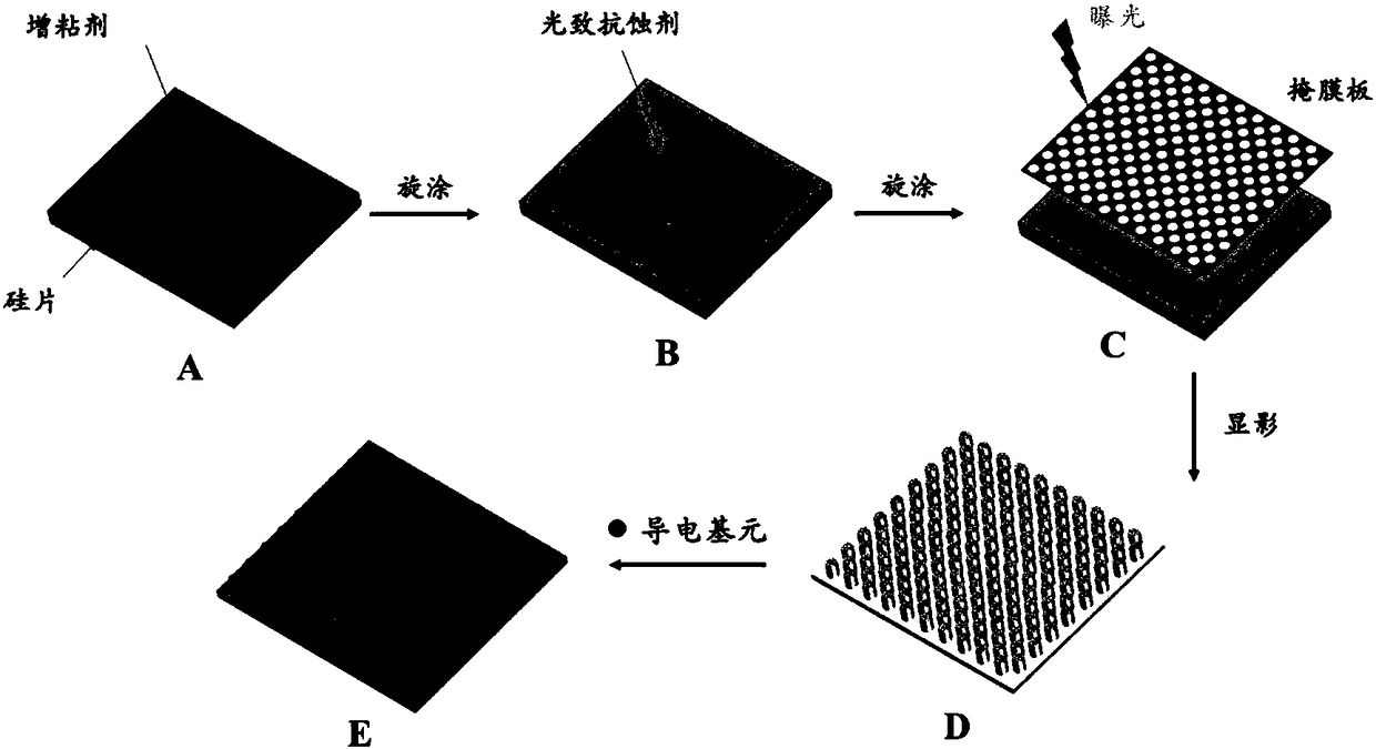
[0044] (1) Fabrication of photolithographic microelectrode arrays

[0045]Spin-coat a layer of adhesion promoter (OMNICOAT) on the silicon wafer after pretreatment, and apply negative photoresist SU-82025 on it after drying, and perform pre-baking, exposure, post-baking, development, and hardening processes to complete the process. The process of transferring the pattern on the mask plate to the surface of the substrate to obtain the required array pattern. The lithography process is:

[0046] Coating film: spin coating method, forward rotation at 600r / min for 10s, back rotation at 2600r / min for 40s, wet film thickness is 50μm;

[0047] Pre-baking: keep in an oven at 65°C for 1min, heat up to 95°C for 6min, then cool down to 65°C for 1min, and let stand for 15min;

[0048] Exposure: Use a mask with a hole diameter and spacing of 50 μm, an exposure wavelength of 365 nm, and a light intensity of 12.9 mw / cm 2 , the time is 9s;

[0049] Post-baking: Keep in an oven at 65°C for...

Embodiment 2

[0057] (1) Fabrication of photolithographic microelectrode arrays

[0058] Spin-coat a layer of adhesion promoter (OMNICOAT) on the silicon wafer after pretreatment, and apply negative photoresist SU-82025 on it after drying, and perform pre-baking, exposure, post-baking, development, and hardening processes to complete the process. The process of transferring the pattern on the mask plate to the surface of the substrate to obtain the required array pattern. The lithography process is:

[0059] Coating film: spin coating method, forward rotation at 600r / min for 10s, back rotation at 4350r / min for 40s, wet film thickness is 20μm;

[0060] Pre-baking: place the photoresist film in an oven at 65°C for 1 minute, raise the temperature to 95°C for 5 minutes, then cool down to 65°C for 1 minute, and let it stand for 15 minutes;

[0061] Exposure: Use a mask with a hole diameter and spacing of 10 μm, an exposure wavelength of 365 nm, and a light intensity of 12.9 mw / cm 2 , the time...

Embodiment 3

[0070] (1) Fabrication of photolithographic microelectrode arrays

[0071] Spin-coat a layer of adhesion promoter (OMNICOAT) on the silicon wafer after pretreatment, and apply negative photoresist SU-82050 on it after drying, and perform pre-baking, exposure, post-baking, development, and hardening processes to complete The process of transferring the pattern on the mask plate to the surface of the substrate to obtain the required array pattern. The lithography process is:

[0072] Coating film: spin coating method, forward rotation at 600r / min for 10s, back rotation at 1000r / min for 40s, wet film thickness is 100μm;

[0073] Pre-baking: place the photoresist film in an oven at 65°C for 5 minutes, raise the temperature to 95°C for 10 minutes, then cool down to 65°C for 1 minute, and let stand for 15 minutes;

[0074] Exposure: Use a mask with a hole diameter and spacing of 5 μm, an exposure wavelength of 365 nm, and a light intensity of 12.9 mw / cm 2 , the time is 11s;

[0...


PUM

PropertyMeasurementUnit
diameteraaaaaaaaaa
thicknessaaaaaaaaaa

Abstract

The invention discloses a preparation method for preparing a microelectrode array based on a photoetching technology and preparing an electrochemical nonenzymatic biosensor by modifying the microelectrode array with a conductive element and an inorganic sensing coating layer, and relates to the field of macromolecular material science, photoetching technologies, electrochemical sensors and the like. Photoresist adopted in the preparation method can realize preparation of the microelectrode array with ultrahigh length-diameter ratio; a three-dimensional structure is developed on the basis of atwo-dimensional planar structure, so that the specific surface area of the coating layer is greatly enlarged, and a foundation is laid for the preparation of a high-sensitivity electrochemical sensor;meanwhile, the three-dimensional microarray structure improves the coarseness of the surface of the coating layer, and the effective load of a sensing coating layer is facilitated. A method for in-situ electrochemical reduction of inorganic transitional metal nano particles in the invention realizes preparation of an inorganic sensing coating layer having an electrochemical response, and has a synergistic effect together with a conductive microelectrode array. The technology disclosed by the invention is easy and convenient to operate; the constructed sensor has the advantages of high sensitivity to an object to be analyzed, high stability and the like.

Description

【Technical field】 [0001] This patent relates to the fields of electrochemical sensors and photoetching, in particular to a method for modifying conductive layers and electrodes of inorganic sensing coatings with photoetched microelectrode arrays as the substrate, and preparing them into enzyme-free biosensors. 【Background technique】 [0002] In recent years, problems such as population aging and chronic diseases have become more and more serious, and early detection and intervention of diseases are particularly important. At the same time, research on various sensor devices has become a hot spot, among which the research on electrochemical sensors is the most concentrated. [0003] An electrochemical sensor is an analytical device that converts biological signals into electrical signals and detects substance concentrations and other biological responses. It is usually composed of identification elements, transducers and signal amplification devices. Electrodes are used as co...

Claims


Application Information

Patent Timeline
Patent Type & Authority Applications(China)
IPC IPC(8): G01N27/26G01N27/30G01N27/48
CPCG01N27/26G01N27/30G01N27/48
Inventor 刘晓亚吴倩许升黄雪雯孙婷婷王满徐梦祎张广俊罗静
Owner JIANGNAN UNIV
Why Eureka
Try Eureka