Quantum well coupling-enhancement ZnO-based light-emitting diode and preparation method thereof
A light-emitting diode, enhanced technology, applied in electrical components, circuits, semiconductor devices, etc., can solve the problems of not further improving luminous efficiency, unfavorable carrier cascade oscillation coupling, reducing luminous efficiency, etc. The effect of adjustable wavelength, high average luminous power and good application prospect
- Summary
- Abstract
- Description
- Claims
- Application Information
AI Technical Summary
Problems solved by technology
Method used
Image
Examples
Embodiment 1
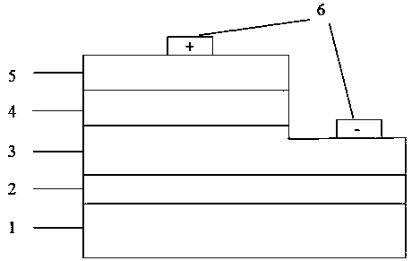
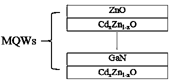
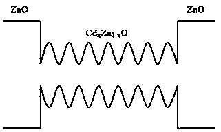
[0044] 1. A quantum well coupling enhanced ZnO-based light-emitting diode, such as figure 1 As shown, including Si substrate 1, buffer layer 2 on the substrate, n-type ZnO layer 3; Cd on the n-type ZnO layer x Zn 1-x O / ZnO multi-quantum well layer 4, p-type ZnO layer 5 on the multi-quantum well layer, metal contact electrode 6 on the p-type ZnO layer and n-type ZnO layer.
[0045] 2. The preparation method of the above-mentioned quantum well coupling enhanced ZnO-based light-emitting diode, the steps are as follows:
[0046] (1) Clean the Si substrate before growth
[0047] The cleaning steps are: first in sulfuric acid (H 2 SO 4 ) and hydrogen peroxide (H 2 o 2 ) for 1 min to 5 min, and then in hydrofluoric acid (HF) for 1 min to 3 min to remove the SiO on the Si surface 2 The oxide layer is corroded away, followed by further ammonia (NH 3 .H 2 O) and hydrogen peroxide (H 2 o 2 ) for 3 min to 15 min, then continue to wash in hydrofluoric acid (HF) for 1 min to 3 mi...
Embodiment 2
[0056] A quantum well coupling enhanced ZnO-based light-emitting diode, its structure and preparation process are the same as in Example 1, the difference is that in the preparation method, buffer layer 2, n-type ZnO layer 3, Cd x Zn 1-x The O / ZnO multiple quantum well layer 4 and the p-type ZnO layer 5 are realized by metal organic vapor deposition (MOCVD).
Embodiment 3
[0058] A quantum well coupling enhanced ZnO-based light-emitting diode, its structure and preparation process are the same as in Example 1, the difference is that in the preparation method, buffer layer 2, n-type ZnO layer 3, Cd x Zn 1-x The O / ZnO multi-quantum well layer 4 and the p-type ZnO layer 5 are realized by means of pulsed laser deposition (PLD).
PUM
| Property | Measurement | Unit |
|---|---|---|
| Thickness | aaaaa | aaaaa |
| Thickness | aaaaa | aaaaa |
| Thickness | aaaaa | aaaaa |
Abstract
Description
Claims
Application Information


