Epitaxial growth method of silicon substrate GaN-based LED

A technology of epitaxial growth and silicon substrate, applied in the direction of crystal growth, single crystal growth, single crystal growth, etc., can solve the problems of epitaxial wafer cracking, large epitaxial layer, large lattice mismatch, etc.

Inactive Publication Date: 2018-06-01
FOSHAN DONGSHEN METAL PROD CO LTD
View PDF0 Cites 4 Cited by
  • Summary
  • Abstract
  • Description
  • Claims
  • Application Information

AI Technical Summary

Problems solved by technology

However, there are still many difficulties in using Si as the substrate. There is a large lattice mismatch between the GaN epitaxial layer and Si crystal, which causes a large number of dislocations in the epitaxial layer; there is also a large thermal mismatch between GaN and Si crystal. At the end of the reaction, from high temperature to room temperature, this thermal mismatch will generate a huge tensile stress in the epitaxial layer, which will cause cracks in the epitaxial wafer.

Method used


Image

  • Epitaxial growth method of silicon substrate GaN-based LED
  • Epitaxial growth method of silicon substrate GaN-based LED
  • Epitaxial growth method of silicon substrate GaN-based LED

Examples


Embodiment Construction

[0013] In order to allow those skilled in the art to understand the present invention more clearly and intuitively, the present invention will be further described below.

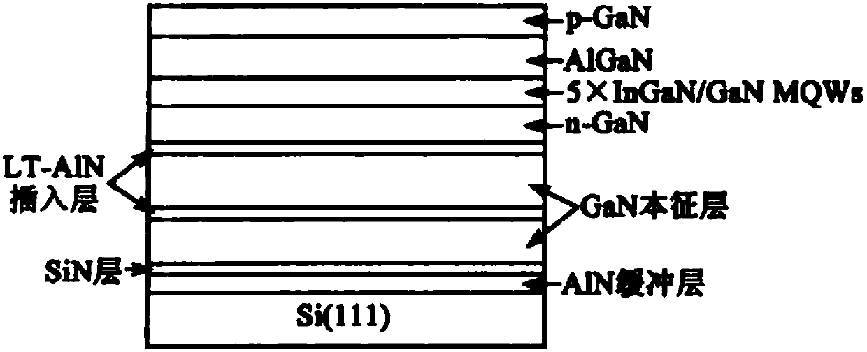
[0014] A GaN-based LED epitaxial growth method on a silicon substrate, using Thomas Swan's LP-MOCVD system, using Si(111) as the substrate, trimethylgallium (TMGa), trimethylaluminum (TMAl), trimethylindium (TMIn) and high-purity NH3 are Ga, Al, In and N sources respectively, H2 and N2 are carrier gases, silane (SiH 4 ) and Magnesium (CP 2 Mg) are n-type and p-type dopants respectively; the Si substrate should be cleaned before growth to remove pollutants and impurities to obtain a clean surface;

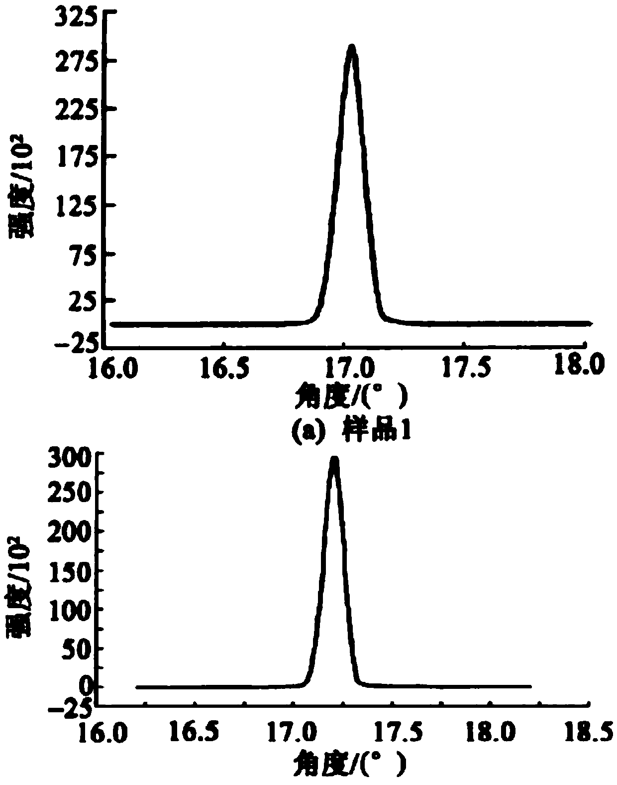
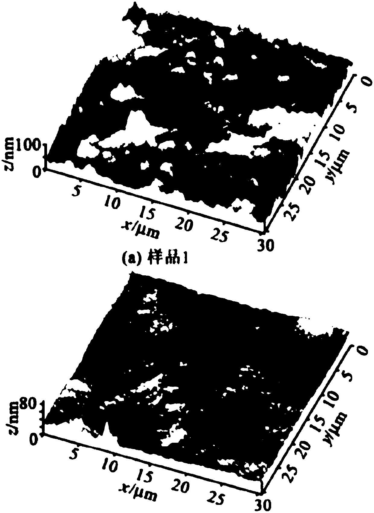
[0015] The epitaxial growth process is as follows: Sample 1 was first grown at 1100 °C, H 2 Hydrogenation under the atmosphere for 10min to clean the surface of the silicon wafer; after hydrogenation treatment, the temperature was lowered to 1060°C to grow the AlN buffer layer and the high-temperature GaN layer...


PUM


Abstract

The invention provides an epitaxial growth method of a silicon substrate GaN-based LED. An LP-MOCVD system of Thomas Swan is adopted, Si (111) is selected as a substrate, TMGa, TMAl, TMIn and high-purity NH3 are respectively sources of Ga, Al, In and N, H2 and N2 are adopted as carrier gases, and SiH4 and CP2Mg are respectively n-type and p-type doping agents; the Si substrate is cleaned before growth to remove pollutants and impurities and obtain a clean surface; and an epitaxial wafer of the silicon substrate GaN-based LED is grown in an epitaxial manner, and the crystallization quality thereof is tested and analyzed by employing DCXRD. It is indicated through a result that the interface of an InGan / GaN multi-quantum well is flat, and the crystallization quality is good; and the period thicknesses of the quantum well, obtained through calculation by employing two methods, are fundamentally consistent.

Description

technical field [0001] The invention relates to a GaN-based LED epitaxial growth method on a silicon substrate. Background technique [0002] Although GaN is an ideal semiconductor device material, there has been a lack of suitable substrates, so good-quality GaN epitaxial layers have not been obtained. Currently, GaN materials used for devices are epitaxially grown through sapphire or SiC substrates. However, these two substrates also have obvious deficiencies. Sapphire is an insulator with high hardness and poor thermal conductivity, making it difficult to process; and SiC is very expensive, which makes the production cost of the device very high. If Si is used as the substrate, it has great advantages over the above two substrate materials, such as large area, low cost, high quality, good electrical and thermal conductivity, etc. Therefore, the research on the growth of GaN thin films on Si substrates has received extensive attention. However, there are still many diffi...

Claims


Application Information

Patent Timeline
IPC IPC(8): H01L33/00H01L33/12H01L33/06C30B25/18C30B29/40
CPCC30B25/183C30B29/406H01L33/007H01L33/06H01L33/12
Inventor 张勇
Owner FOSHAN DONGSHEN METAL PROD CO LTD
Why Eureka
Try Eureka