Semiconductor device and manufacturing method, and electronic device

A manufacturing method and semiconductor technology, applied in the fields of semiconductor/solid-state device manufacturing, semiconductor devices, circuits, etc., can solve the problems of polysilicon damage, active area etching damage, affecting the overall performance and yield of the device, etc. The effect of improving performance and yield, improving margins

Active Publication Date: 2018-06-12
SEMICON MFG INT (SHANGHAI) CORP +1
View PDF3 Cites 7 Cited by
  • Summary
  • Abstract
  • Description
  • Claims
  • Application Information

AI Technical Summary

Problems solved by technology

[0003] During the development of the LDMOS device process, a trench contact (trench CT) process was produced. The trench contact as a shield can improve the breakdown voltage performance of the LDMOS device, and at the same time compared with other shielding methods (such as requiring an additional mask layer To form a metal or polysilicon shielding process), this process can also save a mask layer, but the current trench contact process also encounters various challenges in the implementation, for example, in the trench etching process, It is easy to over-etch the polysilicon gate near the trench, resulting in polysilicon damage, and may even cause etching damage to the active area, thereby affecting the overall performance and yield of the device

Method used


Image

  • Semiconductor device and manufacturing method, and electronic device
  • Semiconductor device and manufacturing method, and electronic device
  • Semiconductor device and manufacturing method, and electronic device

Examples


Embodiment 1

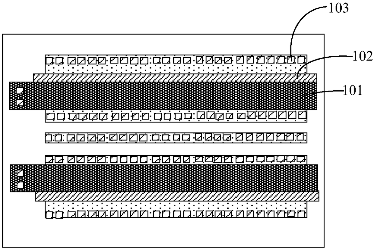
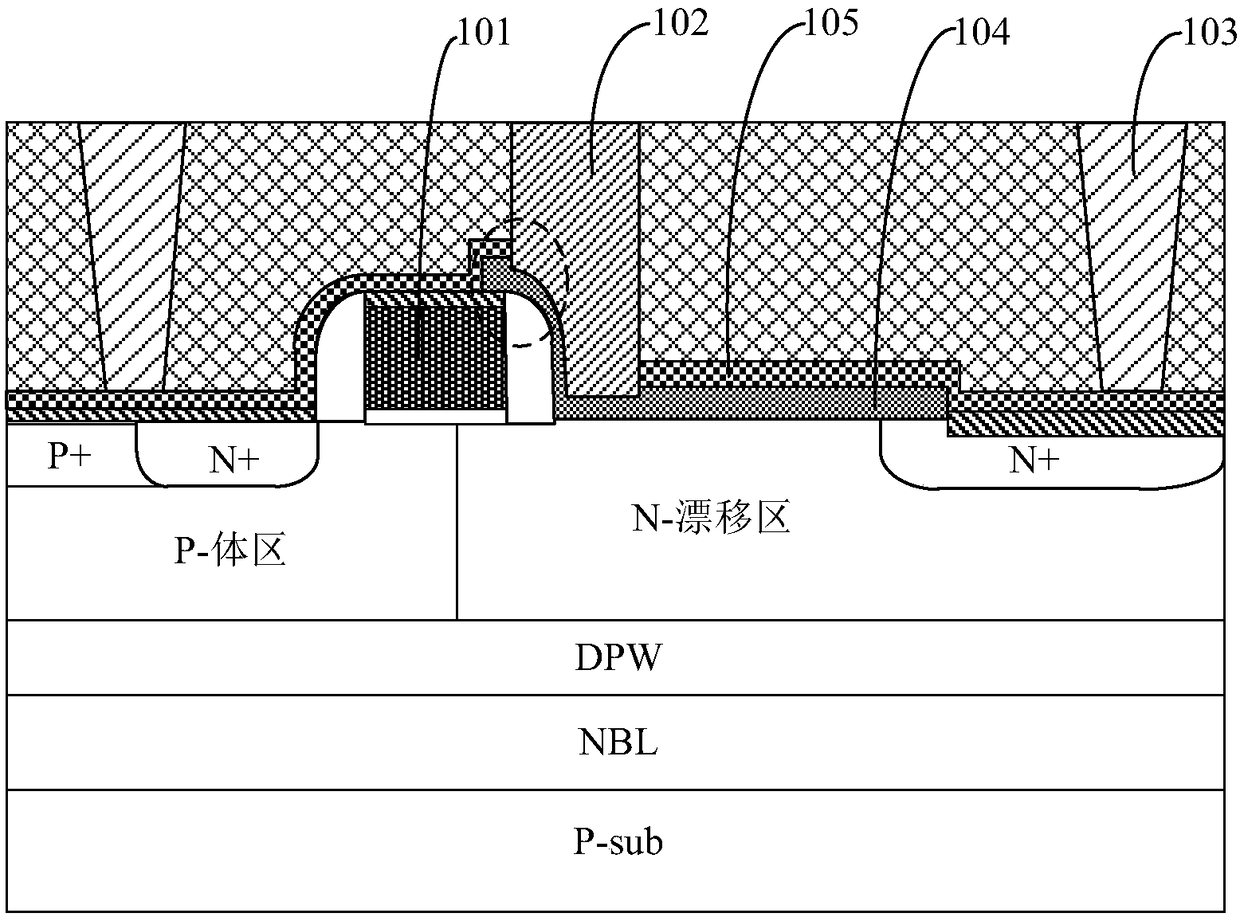
[0070] In order to solve the above technical problems, the present invention provides a semiconductor device, such as image 3 shown, which includes:

[0071] a semiconductor substrate of the first conductivity type;

[0072] a gate structure formed on the semiconductor substrate;

[0073] A source and a drain are formed in the semiconductor substrate on both sides of the gate structure, there is a space between the drain and the gate structure, and a connection line between the source and the drain is defined The extending direction is the first direction;

[0074] a trench contact formed on the semiconductor substrate between the gate structure and the drain, wherein the trench contact includes a body portion and several Comb teeth, the main body part is provided with the comb teeth along at least one side in the first direction.

[0075] The trench contact of the semiconductor device of the present invention includes a main body and several comb teeth connected to the m...

Embodiment 2

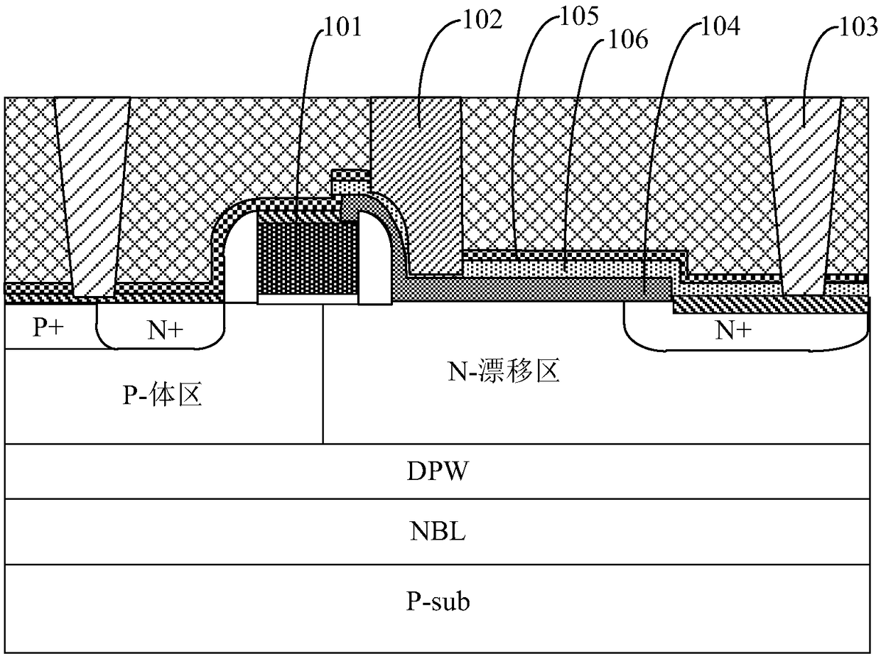
[0125]The present invention also provides a method for manufacturing the semiconductor device in the aforementioned implementation one, such as image 3 As shown, it mainly includes the following steps:

[0126] Step S1, providing a semiconductor substrate of the first conductivity type;

[0127] Step S2, forming a gate structure on the semiconductor substrate;

[0128] Step S3, forming a source and a drain in the semiconductor substrate on both sides of the gate structure, wherein there is a gap between the drain and the gate structure, defining a gap between the source and the drain The extension direction of the connecting line is the first direction;

[0129] Step S4, forming a trench contact on the semiconductor substrate between the gate structure and the drain, wherein the trench contact includes a body part and several comb teeth connected to the body part, The main body portion is provided with the comb teeth along at least one side in the first direction.

[0130...

Embodiment 3

[0192] The present invention also provides an electronic device, including the semiconductor device described in Embodiment 1, or the semiconductor device prepared by using the manufacturing method described in Embodiment 2.

[0193] The electronic device of this embodiment can be any electronic device such as a mobile phone, a tablet computer, a notebook computer, a netbook, a game console, a TV set, a VCD, a DVD, a navigator, a digital photo frame, a camera, a video camera, a recording pen, MP3, MP4, PSP, etc. Product or equipment, but also any intermediate product including electrical circuits. The electronic device according to the embodiment of the present invention has better performance due to the use of the above-mentioned semiconductor device.

[0194] in, Figure 4 An example of a mobile phone handset is shown. The mobile phone handset 400 is provided with a display portion 402 included in a housing 401, operation buttons 403, an external connection port 404, a spe...


PUM


Abstract

The invention provides a semiconductor device and a manufacturing method, and an electronic device and relates to the semiconductor technology field. The semiconductor device comprises the first conductive type of a semiconductor substrate, a grid structure, a source electrode and a drain electrode, and a groove contact, wherein the grid structure is formed on the semiconductor substrate; the source electrode and the drain electrode are formed in the semiconductor substrate of the two sides of the grid structure, an interval exists between the drain electrode and the grid structure, and the extension direction of a connection line between the source electrode and the drain electrode is defined as a first direction; the groove contact is formed in the semiconductor substrate between the grid structure and the drain electrode; the groove contact includes a main body portion and several comb teeth connected to the main body portion; and the at least one side of the main body portion, which is along with the first direction, is provided with the comb teeth. By using the groove contact of the semiconductor device, the margin of a manufacturing technology can be improved, the key size ofthe groove contact can be reduced, and a problem that an active area and a polycrystalline silicon grid are damaged during groove contact manufacturing can be effectively solved.

Description

technical field [0001] The present invention relates to the technical field of semiconductors, in particular to a semiconductor device, a manufacturing method thereof, and an electronic device. Background technique [0002] LDMOS (Laterally Diffused Metal Oxide Semiconductor; laterally diffused metal oxide semiconductor), as one of the important components of power devices, has broad application prospects. Since LDMOS devices are usually used in power circuits, such as RF technology and power MOSFET devices, power circuits need to obtain high-voltage power amplification and large output power, so LDMOS devices must be able to withstand higher voltages. As LDMOS is widely used in power integrated circuits, the requirements for the performance of LDMOS devices are getting higher and higher, which requires a higher breakdown voltage (BV) of LDMOS devices, and may also require an increase in threshold drift. In conclusion, the demand for LDMOS devices with higher breakdown volt...

Claims


Application Information

Patent Timeline
Patent Type & Authority Applications(China)
IPC IPC(8): H01L29/78H01L21/336
CPCH01L29/66681H01L29/7816
Inventor 伏广才
Owner SEMICON MFG INT (SHANGHAI) CORP
Why Eureka
Try Eureka