
A silicon carbide power semiconductor device with low on-resistance

A technology of power semiconductors and low on-resistance, applied in semiconductor devices, electrical components, circuits, etc., can solve the problem of high on-resistance, achieve reduced on-resistance, high current capability, lower on-resistance and threshold voltage Effect

Active Publication Date: 2021-07-13
SOUTHEAST UNIV +1
View PDF0 Cites 0 Cited by
  • Summary
  • Abstract
  • Description
  • Claims
  • Application Information

AI Technical Summary

Problems solved by technology

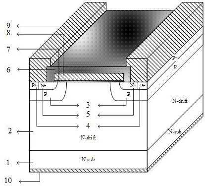
However, since the conductive channel of the conventional silicon carbide power semiconductor device is close to the bottom of the gate oxide layer, the defects on the surface of the gate oxide layer will affect the carrier transport, so the conventional silicon carbide power semiconductor device has a high on-resistance

Method used


Image

  • A silicon carbide power semiconductor device with low on-resistance
  • A silicon carbide power semiconductor device with low on-resistance
  • A silicon carbide power semiconductor device with low on-resistance

Examples


Embodiment Construction

[0022] The present invention will be described in detail below in conjunction with the accompanying drawings.

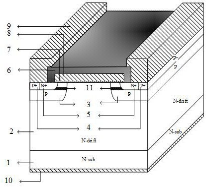
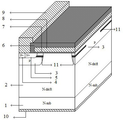
[0023] refer to figure 2 , a silicon carbide power semiconductor device with low on-resistance, the silicon carbide power semiconductor device with low on-resistance is an axisymmetric structure, comprising: an N-type substrate 1 connected to one side of the N-type substrate 1 The drain metal 10 is provided with an N-type drift region 2 on the other side of the N-type substrate 1, a pair of P-type base regions 3 are symmetrically arranged in the N-type drift region 2, and a pair of P-type base regions 3 are arranged in each P-type base region 3 respectively. There are P+ type body contact regions 4 and N+ type source regions 5, a gate oxide layer 7 is provided on the surface of the N type drift region 2, a polysilicon gate 8 is provided on the surface of the gate oxide layer 7, and a passivation layer is provided on the polysilicon gate 8. and the passivation layer...


PUM

PropertyMeasurementUnit
thicknessaaaaaaaaaa

Abstract

A silicon carbide power semiconductor device with low on-resistance, the silicon carbide power semiconductor device with low on-resistance is an axisymmetric structure, comprising: an N-type substrate, and an N-type drift region is arranged on the N-type substrate A pair of P-type base regions are symmetrically arranged in the N-type drift region, a P+ type body contact region and an N+ type source region are arranged in the P-type base region, and a gate oxide layer is arranged on the surface of the N-type drift region. The surface of the oxygen layer is provided with a polysilicon gate. It is characterized in that: an array composed of N-type regions is provided in the body of the P-type base region, and the upper surface is separated from the gate oxide layer, and the N-type regions are separated from the P-type region in the gate width direction of the device. The regions are distributed at intervals, and the distance, thickness and doping concentration from the N-type region to the gate oxide layer make the N-type region just completely pinch off in a natural state. The advantage of this structure is that while maintaining the breakdown voltage of the device, it can effectively reduce the on-resistance of the device, improve the on-state current capability of the device, and reduce the on-state energy loss.

Description

technical field [0001] The present invention mainly relates to the field of high-voltage power semiconductor devices, specifically, a silicon carbide power semiconductor device with low on-resistance, suitable for high-temperature, high-frequency, high-power applications in aerospace, aviation, oil exploration, nuclear energy, radar and communications, etc. , Strong radiation and other extreme environments coexist. Background technique [0002] Silicon carbide is one of the wide bandgap semiconductor materials developed rapidly in the past ten years. Compared with the widely used semiconductor materials silicon, germanium and gallium arsenide, silicon carbide has the advantages of wide bandgap, high breakdown electric field, high carrier saturation drift rate, high thermal conductivity and high power density. Ideal material for high-power, high-frequency devices. At present, developed countries such as the United States, Europe, and Japan have basically solved the problems...

Claims


Application Information

Patent Timeline
Patent Type & Authority Patents(China)
IPC IPC(8): H01L29/78H01L29/10
CPCH01L29/1095H01L29/7802
Inventor 刘斯扬李婷魏家行李智超方炅孙伟锋陆生礼时龙兴
Owner SOUTHEAST UNIV
Learn More