Patterning methods for nanomaterials

A nanomaterial and patterning technology, applied in nanotechnology, printing, printing devices, etc., can solve the problems of difficulty in patterning methods, waste of raw materials, inability to accurately control the deposition amount of nanomaterials, etc., and achieve the effect of improving the quality of patterning

Active Publication Date: 2019-07-05
SUZHOU INST OF NANO TECH & NANO BIONICS CHINESE ACEDEMY OF SCI
View PDF4 Cites 2 Cited by
  • Summary
  • Abstract
  • Description
  • Claims
  • Application Information

AI Technical Summary

Problems solved by technology

[0003] In the process of research and use of nanomaterials, how to effectively realize its patterning is the key to determine the application of nanomaterials, but for sheet-like two-dimensional materials and one-dimensional nanowire materials with high aspect ratio, the patterning method is relatively difficult
At present, the existing methods mainly include the following: one is the method of inkjet printing (ACS Appl.Mater.Interfaces, 2015, 7(17), pp 9254–9261). For the printing of sheet-like graphene or linear nanowire materials, it is difficult to achieve high-quality patterning due to the limitations of the nozzle (sheet-like two-dimensional materials and linear one-dimensional materials are difficult to print through inkjet nozzles) ; One is through photolithography or laser cutting (ACSAppl.Mater.Interfaces2015, 7, 13467-13475; Nanoscale, 2014, 6, 946–952), photolithography and laser cutting itself are a very mature patterning method , but they are all subtractive processing processes, which have the disadvantages of destroying the structure of nanomaterials and wasting raw materials, and the flatness of the cutting edge is very difficult to control; there is also a method of electrostatic spraying (ACS Appl.Mater.Interfaces 2015 , 7, 14272-14278), electrostatic spraying itself is a method of uniform film formation, but patterning requires the use of masks, and electrostatic spraying itself cannot accurately control the deposition amount of nanomaterials per unit area of ​​the surface, so it is not An effective method for patterning sheet-like 2D materials and 1D materials with high aspect ratio

Method used


Image

  • Patterning methods for nanomaterials
  • Patterning methods for nanomaterials
  • Patterning methods for nanomaterials

Examples


Embodiment 1

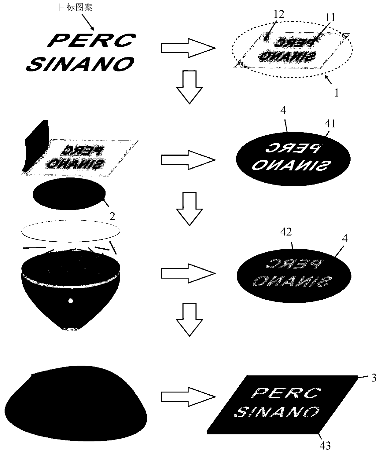
[0037] Firstly, the pattern of the screen plate 1 is customized. In this embodiment, the target pattern is three simple geometric figures of triangle, circle and square. Then, on the surface of the filter membrane 2 covered with the screen plate 1, the polymer slurry is screen-printed, wherein the material of the filter membrane 2 is polytetrafluoroethylene, and the diameter of the filter membrane 2 is 50mm, and the micropores on the filter membrane 2 are The pore size is 0.2 μm, and the polymer slurry is polydimethylsiloxane (PDMS, 10:1). Heat and solidify rapidly at a temperature of 80° C. to obtain a patterned polymer paste layer 4 .

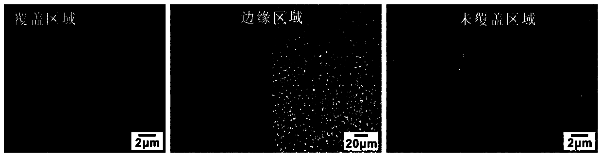
[0038] figure 2 Shown is the scanning electron microscope (SEM) image of different regions after screen printing PDMS on the surface of filter membrane 2. It can be seen that the PDMS uncovered area on filter membrane 2 maintains the original pore structure, and the boundary between the uncovered area and the covered area The edge area is ...

Embodiment 2

[0044] The difference between embodiment 2 and embodiment 1 is that the filter membrane 2 is made of nylon, the nanomaterial is carbon nanotube (CNT), and the substrate 3 is polyethylene terephthalate (PET) film.

[0045] Image 6 Shown is the SEM image of the microelectrode made of CNT.

Embodiment 3

[0047] Embodiment 3 differs from Embodiment 1 in that the material of the filter membrane 2 is polyvinylidene fluoride, the diameter of the filter membrane 2 is 100 mm, the nanomaterial is graphene, and the substrate 3 is a silica gel film.

[0048] Figure 7 Shown is the SEM picture of the microelectrode made of graphene.

[0049] It can be understood that, in other embodiments, the filter membrane 2, the polymer slurry and the substrate 3 can be made of other materials, which are not limited here. Of course, other sheet-like two-dimensional materials or wire-like one-dimensional materials can also be used as nanomaterials. The graphene, carbon nanotubes, and silver nanowires given in this embodiment are only shown as examples and are not intended to be limiting.


PUM


Abstract

The invention discloses a method for patterning nanometer materials. The patterning method includes the following steps: providing a net plate, a filter membrane and a substrate; covering the net plate on the filter membrane; Printing polymer slurry to form a patterned polymer slurry layer on the surface of the filter membrane; depositing nanomaterials on the patterned area of ​​the polymer slurry layer to form a nanomaterial structure; The structure is transferred onto the substrate. In the method for patterning nanomaterials provided by the present invention, an imaged polymer slurry layer is formed by screen printing, and then nanomaterials are deposited on the patterned region of the polymer slurry layer to form a patterned nanomaterial structure; Finally, the nanomaterial structure is transferred onto the substrate. The imaging method can effectively realize the patterning of nanomaterials and improve the patterning quality of nanomaterials.

Description

technical field [0001] The invention relates to the technical field of patterning of nanomaterials, in particular to a patterning method of nanomaterials. Background technique [0002] Due to its special nano-effects, nanomaterials have been increasingly used in various fields of science and engineering in recent years. Common nanomaterials include graphene, silver nanowires, and carbon nanotubes. Graphene is a new type of nanomaterial with the thinnest, strongest, and strongest electrical and thermal conductivity found so far. It is regarded as the most potential substitute for silicon materials. It is used to manufacture ultra-miniature transistors and produce future supercomputers. Silver nanowires are one-dimensional nanomaterials with a high aspect ratio, and are considered to be the most likely material to replace traditional ITO transparent electrodes. It provides the possibility to realize flexible and bendable LED displays, touch screens, etc. A large number of st...

Claims


Application Information

Patent Timeline
Patent Type & Authority Patents(China)
IPC IPC(8): B41M1/12B82Y40/00
CPCB41M1/12B82Y40/00
Inventor 袁伟崔铮顾唯兵林剑
Owner SUZHOU INST OF NANO TECH & NANO BIONICS CHINESE ACEDEMY OF SCI
Why Eureka
Try Eureka