PCB (printed circuit board) resistance welding pretreatment process

A pretreatment and process technology, applied in the field of PCB solder mask pretreatment process, can solve the problems of insufficient copper surface layer and hole roughness, affecting PCB assembly, and high labor costs, reducing the probability of scratches on the board surface, improving The effect of processing efficiency and labor cost reduction

Active Publication Date: 2018-07-13
江西景旺精密电路有限公司
View PDF6 Cites 7 Cited by
  • Summary
  • Abstract
  • Description
  • Claims
  • Application Information

AI Technical Summary

Problems solved by technology

[0004] The traditional pre-treatment method of solder mask is to use a combination of mechanical brushing and chemical micro-etching to process the board surface, but this method does not roughen the copper surface and holes of the PCB enough. Once the thick copper foil circuit board is made At this time, the bonding force between the ink and the copper layer is relatively weak, which causes the solder resist ink to easily foam and fall off, which affects the subsequent PCB assembly
In addition, in the board receiving process in the traditional solder mask pretreatment method, the PCB boards that have passed the solder mask pretreatment line must be stored in the rack, that is, each board must be processed with the rack board, and the operator is 25 per rack. One board needs to be transported once, and the operation procedures such as inserting racks and transporting are cumbersome, labor-intensive, high labor costs, and low production efficiency

Method used


Image

  • PCB (printed circuit board) resistance welding pretreatment process

Examples


Embodiment 1

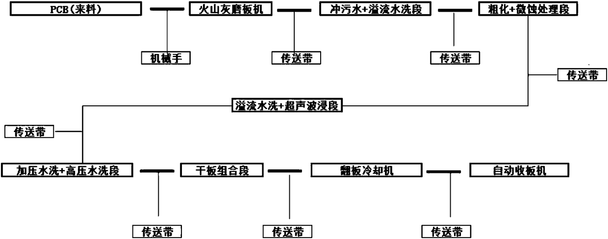
[0029] This embodiment provides a pre-treatment process for PCB solder mask, such as figure 1 As shown, it includes the following steps:

[0030] S1. Automatic feeding. The PCB boards to be processed are stored in a temporary feeding storage rack, and the manipulator is controlled to grab and transport the PCB boards to be processed stored in the temporary feeding storage rack to the feeding end of the volcanic ash grinding machine.

[0031] S2, volcanic ash grinding plate treatment, the volcanic ash grinding machine has a nylon grinding wheel, and the nylon grinding wheel rotates at a high speed to spray the mixture of volcanic ash and water onto the surface of the PCB board. The volcanic ash can be selected from No. 325-400 volcanic ash, this embodiment The volume percentage of medium volcanic ash in the volcanic ash-water mixture is 12% (V / V), and the width of the wear marks on the board surface controlled by the volcanic ash is 8mm. Spray the volcanic ash-water mixture on ...

Embodiment 2

[0037] This embodiment provides a pre-treatment process for PCB solder mask, such as figure 1 As shown, it includes the following steps:

[0038] S1. Automatic feeding. The PCB boards to be processed are stored in a temporary feeding storage rack, and the manipulator is controlled to grab and transport the PCB boards to be processed stored in the temporary feeding storage rack to the feeding end of the volcanic ash grinding machine.

[0039] S2, volcanic ash grinding plate treatment, the volcanic ash grinding machine has a nylon grinding wheel, and the nylon grinding wheel rotates at a high speed to spray the mixture of volcanic ash and water onto the surface of the PCB board. The volcanic ash can be selected from No. 325-400 volcanic ash, this embodiment The volume percentage of medium volcanic ash in the volcanic ash-water mixture is 16% (V / V), and the width of the wear marks on the board surface controlled by the volcanic ash is 10mm. Spray the volcanic ash-water mixture on...

Embodiment 3

[0045] This embodiment provides a pre-treatment process for PCB solder mask, such as figure 1 As shown, it includes the following steps:

[0046] S1. Automatic feeding. The PCB boards to be processed are stored in a temporary feeding storage rack, and the manipulator is controlled to grab and transport the PCB boards to be processed stored in the temporary feeding storage rack to the feeding end of the volcanic ash grinding machine.

[0047] S2, volcanic ash grinding plate treatment, the volcanic ash grinding machine has a nylon grinding wheel, and the nylon grinding wheel rotates at a high speed to spray the mixture of volcanic ash and water onto the surface of the PCB board. The volcanic ash can be selected from No. 325-400 volcanic ash, this embodiment The volume percentage of medium volcanic ash in the volcanic ash-water mixture is 20% (V / V), and the width of the wear marks on the surface of the volcanic ash is controlled to be 12mm. The volcanic ash-water mixture is spray...


PUM


Abstract

The invention discloses a PCB (printed circuit board) resistance welding pretreatment process. The PCB resistance welding pretreatment process includes the steps of automatic feeding, volcanic-ash board grinding, roughening, microetching, surface cleaning, board drying, cooling and automatic board collecting. The process is high in automation degree, feeding and receiving are operated automatically, the step of carrying boards manually is omitted, processing efficiency is improved, and labor cost is lowered; in the steps of roughening and microetching, copper surfaces and holes of the PCBs aretreated by adopting a roughening solution and a microetching solution, the copper surface roughening effect is controlled by controlling of copper surface roughness and cleanliness, the roughness anduniformity of the copper surfaces can be optimized by roughening and microetching treatment, the binding force of the copper surfaces and the holes of the PCBs with resistance welding ink is improved, problems of bubbling and ink coming off the resistance welding layer are solved, and in addition, automatic board collecting operation also reduces the probability of friction on the board surfaces.

Description

technical field [0001] The invention belongs to the technical field of printed circuit board production, and relates to a printed circuit board solder resistance treatment process, in particular to a PCB solder resistance pretreatment process. Background technique [0002] A printed circuit board (Printed Circuit Board, PCB) is a mechanical support for the fixed assembly of various electronic components such as integrated circuits, and realizes wiring and electrical connections or electrical insulation between various electronic components such as integrated circuits. 1. A product that provides the required electrical characteristics (such as characteristic impedance, etc.). Printed circuit boards are generally composed of pads, vias, soldering layers, silk screen layers, copper wires, and various components. Usually, in order to increase the thickness of the copper skin, the green oil is removed by scribing on the solder mask layer, and then Adding tin achieves the effect ...

Claims


Application Information

Patent Timeline
Patent Type & Authority Applications(China)
IPC IPC(8): H05K3/28
CPCH05K3/28H05K2203/14
Inventor 管术春段绍华柯勇何小强
Owner 江西景旺精密电路有限公司
Why Eureka
Try Eureka