Preparation method of grid enhanced gallium nitride field effect device with P type 2D material

A two-dimensional material and gallium nitride field technology, which is applied in semiconductor/solid-state device manufacturing, semiconductor devices, electrical components, etc., can solve problems such as lattice damage, difficulty in precise control, and surface current of damaged barrier layers, so as to improve device performance. Reliability, reducing gate leakage, improving the effect of current collapse

Active Publication Date: 2018-08-03
BEIJING HUATAN TECH CO LTD
View PDF4 Cites 6 Cited by
  • Summary
  • Abstract
  • Description
  • Claims
  • Application Information

AI Technical Summary

Problems solved by technology

[0005] However, due to the inherent limitations of these methods, such as difficult operation and poor repeatability, it is difficult for the above methods to be widely used.
For example, the etching process of the concave gate groove is difficult to control accurately, and at the same time, it will damage the surface of the barrier layer and cause the problem of current co

Method used


Image

  • Preparation method of grid enhanced gallium nitride field effect device with P type 2D material
  • Preparation method of grid enhanced gallium nitride field effect device with P type 2D material
  • Preparation method of grid enhanced gallium nitride field effect device with P type 2D material

Examples


Embodiment Construction

[0032] The technical solutions in the embodiments of the present invention will be clearly and completely described below in conjunction with the drawings in the embodiments of the present invention.

[0033] Figure 1-Figure 7 It is a flowchart of a method for manufacturing a P-type two-dimensional material gate-enhanced gallium nitride field effect device according to an embodiment of the present invention, which specifically includes the following steps:

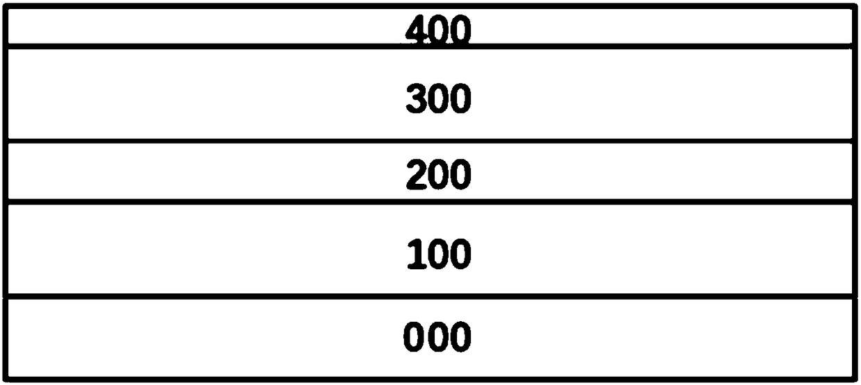
[0034] Step 1) epitaxy the AlGaN buffer layer 100, the GaN channel layer 200, the AlGaN barrier layer 300, and the GaN interface control layer 400 sequentially on the single crystal substrate 000, such as figure 1 shown.

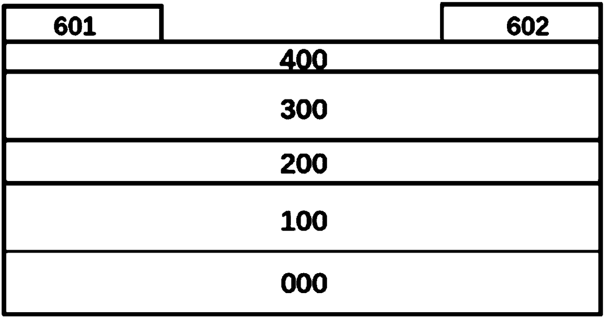
[0035] Step 2) Deposit Ti / TiN / Al source and drain metals 601, 602 to form ohmic contacts through superalloys, such as figure 2 shown.

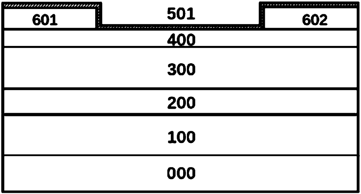
[0036] Step 3) epitaxy the P-type WSe by CVD above the GaN interface control layer 2 Layer 501, such as image 3 shown.

[0037] Step 4) Defining the gate metal ...


PUM

PropertyMeasurementUnit
Thicknessaaaaaaaaaa

Abstract

The invention provides a preparation method of a grid enhanced gallium nitride field effect device with a P type 2D material. The method comprises the following steps that a buffer layer, a channel layer, a barrier layer and an interface control layer are arranged on a monocrystalline substrate successively in an epitaxy way to obtain an epitaxial substrate; source and drain metal are deposited insource and drain regions on the epitaxial substrate respectively to form ohmic contact; a 2D material layer is deposited on the epitaxial substrate; a grid metal region is defined, and grid metal isdeposited; and the 2D material between the grid and source and between the grid and drain is oxidized in the oxygen rich atmosphere; a medium passivation layer is deposited in the surface of the interface control layer; and contact holes between the source/drain and the grid are formed. The P type 2D material replaces a traditional P-GaN layer, and exhaust 2D electron gas thereunder to form an enhanced filed effect ransistor, etching is replaced by oxidation, damage on the surface of a barrier layer can be reduced, and difficulties in the prior art are overcome.

Description

technical field [0001] The invention relates to the field of semiconductor device manufacture, in particular to a preparation method of a P-type two-dimensional material gate enhanced gallium nitride field effect device. Background technique [0002] GaN materials have the characteristics of large band gap, high critical breakdown electric field, and high thermal conductivity, and have broad application prospects in broadband communications, power electronics, and other fields. [0003] Due to the spontaneous polarization and piezoelectric polarization effects at the interface between gallium nitride (GaN) and aluminum gallium nitride (AlGaN) heterojunction, the two-dimensional electron gas concentration is very high (>1E13cm -2 ), which makes GaN FETs [here FETs refer to HEMT (High Electron Mobility Transistor) devices] have very low on-resistance and switching delay. However, the high concentration of two-dimensional electron gas at the AlGaN / GaN heterointerface makes ...

Claims


Application Information

Patent Timeline
IPC IPC(8): H01L29/778H01L29/06H01L21/335
CPCH01L29/06H01L29/66045H01L29/778
Inventor 梁世博
Owner BEIJING HUATAN TECH CO LTD
Why Eureka
Try Eureka