Reverse electric conduction structure of double-surface solar cell based on PERC and manufacturing method

A technology of double-sided solar cells and conductive structures, applied in circuits, photovoltaic power generation, electrical components, etc., can solve problems such as low photoelectric conversion efficiency, improve photoelectric conversion efficiency, improve the ability to export photogenerated carriers, and reduce heat The effect of loss on power loss

Pending Publication Date: 2018-08-03
TONGWEI SOLAR ENERGY CHENGDU CO LID
View PDF0 Cites 13 Cited by
  • Summary
  • Abstract
  • Description
  • Claims
  • Application Information

AI Technical Summary

Problems solved by technology

[0004] The purpose of the present invention is to provide a PERC-based double-sided solar cell rear conductive structure and manufacturing

Method used


Image

  • Reverse electric conduction structure of double-surface solar cell based on PERC and manufacturing method
  • Reverse electric conduction structure of double-surface solar cell based on PERC and manufacturing method
  • Reverse electric conduction structure of double-surface solar cell based on PERC and manufacturing method

Examples


Embodiment 1

[0040] The manufacturing process of PERC-based bifacial solar cells with five busbar structures is as follows:

[0041] 1) P-type monocrystalline silicon wafers are cleaned to remove impurities and surface defects, and double-sided textured to form a 2-6um random pyramid textured surface.

[0042] 2) Back-to-back diffusion, negative pressure diffusion phosphorus source on the front side of the silicon wafer to prepare 0.3um deep PN junction.

[0043] 3) Remove the PSG on the front side, remove the excess diffused PN junction at the side boundary, and properly polish and correct the suede 2-4um on the back side.

[0044] 4) Double-sided oxidation and annealing to form a 3-7nm silicon dioxide film.

[0045] 5) ALD reaction deposition of Al with a film thickness of 4-6nm on the back surface 2 o 3 film.

[0046] 6) Double-sided PECVD reaction deposition of Si 3 N 4 For the thin film, a silicon nitride anti-reflection passivation protective film of 75-90nm is deposited on the...

Embodiment 2

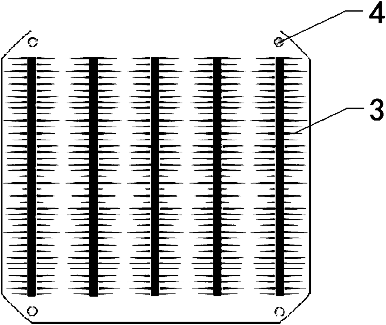
[0053] On the basis of Embodiment 1, the silver paste printing pair with the same pattern and a diameter of 0.3 mm is marked on the corresponding position of the silver bus grid electrode screen with a length of 155.5 mm and a width of 0.8 mm on the back side of the silver bus grid electrode 8. Fitting point 1, and make the center of the alignment fitting point 1 printed with silver paste and the alignment fitting point 5 printed with aluminum paste concentric, and the center of the alignment fitting point 1 printed with silver paste is located in the extended area of ​​the silver bus grid electrode area 2 on the coverage area. Then, the silver paste printing machine captures the aluminum paste printing alignment fitting point 5 marked by the aluminum paste printing machine, and the CCD camera of the silver paste printing machine adjusts the X, Y and angle of the screen to make the silver paste printing alignment fitting point 5 The center of joint point 1 is aligned with the ...


PUM

PropertyMeasurementUnit
Line widthaaaaaaaaaa
Line lengthaaaaaaaaaa

Abstract

The invention discloses a reverse electric conduction structure of a double-surface solar cell based on PERC and a manufacturing method. The structure comprises a reverse passivation film layer, a reverse silver main grid electrode is arranged on the reverse passivation film layer, and laser grooving areas are arranged at the two sides of the reverse silver main grid electrode; the widths of the laser grooving areas are gradually narrowed in the direction away from the reverse silver main grid electrode. The manufacturing method comprises the steps that S1, a silver main grid electrode area isreserved on the reverse passivation film layer, and the laser grooving areas and counterpoint embedding points are arranged on the reverse passivation film layer; S2, by using the counterpoint embedding points, aluminum grid lines are printed on the laser grooving areas; S3, by using the counterpoint embedding points, the reverse silver main grid electrode and silver grid lines are printed on analuminum grid layer. The reverse electric conduction structure and the manufacturing method have the advantages that by means of a tapered structure of gradual widening, the capacity of exporting reverse photon-generated carriers along local grid lines is improved, thermal loss and power loss in the exporting process are reduced, and the photoelectric conversion efficiency of front and reverse surfaces of the double-surface solar cell based on PERC is improved.

Description

technical field [0001] The invention belongs to the field of crystalline silicon solar cell manufacturing, and in particular relates to a PERC-based double-sided solar cell back conductive structure and a manufacturing method. Background technique [0002] Passivated Emitter Rear Contact (PERC) solar cells are a new generation of high-efficiency battery devices. Compared with traditional aluminum back-field solar cells, PERC cells can significantly improve the photoelectric conversion efficiency of the cell. Based on the PERC cell technology, a PERC+ double-sided solar cell is derived by printing partial aluminum grid lines instead of all-aluminum printing in the screen printing process. PERC+ double-sided solar cells can reduce the amount of aluminum paste used, and at the same time can improve the warpage stress of the battery sheet, and reduce the fragmentation rate caused by warpage stress in the welding process of the battery package assembly. Since the PERC+ double-si...

Claims


Application Information

Patent Timeline
IPC IPC(8): H01L31/0224H01L31/18
CPCH01L31/022441H01L31/1804Y02E10/547Y02P70/50
Inventor 王岚吴俊旻张冠纶常青洪布双张鹏谢耀辉
Owner TONGWEI SOLAR ENERGY CHENGDU CO LID
Why Eureka
Try Eureka