P-type gate enhanced transistor based on oxidation self-stop technology and preparation method thereof

A self-stopping and enhanced technology, applied in semiconductor/solid-state device manufacturing, semiconductor devices, electrical components, etc., can solve the problems that cannot meet the urgent needs of high frequency, low loss and high power capacity of the power system, and achieve current suppression Collapse, avoid interface states, and improve device performance

Inactive Publication Date: 2018-08-17
SUZHOU INST OF NANO TECH & NANO BIONICS CHINESE ACEDEMY OF SCI
View PDF3 Cites 7 Cited by
  • Summary
  • Abstract
  • Description
  • Claims
  • Application Information

AI Technical Summary

Problems solved by technology

With the rapid development of power electronics technology, the limitations of traditional silicon materials and second-generation semiconductor materials have become increasingly prom

Method used


Image

  • P-type gate enhanced transistor based on oxidation self-stop technology and preparation method thereof
  • P-type gate enhanced transistor based on oxidation self-stop technology and preparation method thereof
  • P-type gate enhanced transistor based on oxidation self-stop technology and preparation method thereof

Examples


preparation example Construction

[0039] An embodiment of the present invention provides a method for preparing a p-type gate enhancement transistor based on oxidation self-stop technology, including:

[0040] providing a heterojunction comprising a first semiconductor and a second semiconductor, the second semiconductor being formed on the first semiconductor and having a bandgap wider than that of the first semiconductor, the heterojunction having two-dimensional electrons formed therein gas;

[0041] sequentially growing a third semiconductor and a fourth semiconductor on the heterojunction;

[0042] placing a mask over the fourth semiconductor, and oxidizing the fourth semiconductor exposed from the mask to form an oxide, and self-stopping the oxidation reaction upon reaching the third semiconductor; and

[0043] making the source, drain and gate, so that the gate is connected to the fourth semiconductor remaining in the region under the gate, the source and the drain can be connected through the two-dime...

Embodiment 1

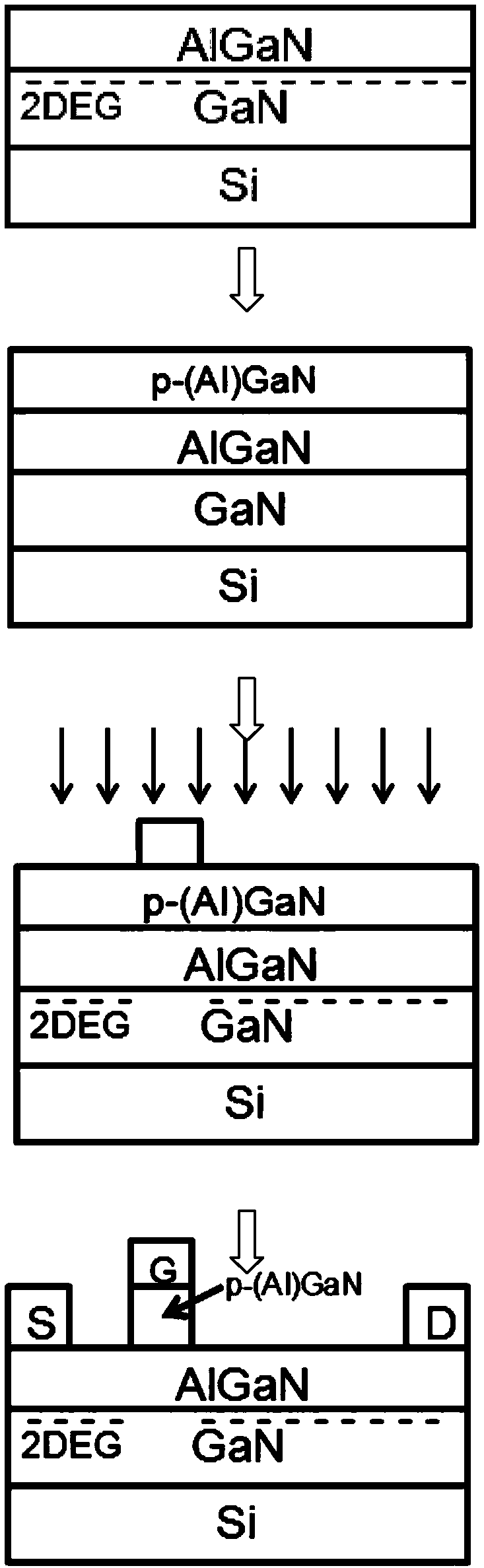
[0079] The preparation method of the p-type gate enhancement transistor based on oxidation self-stop technology provided by the present invention may include the following steps:

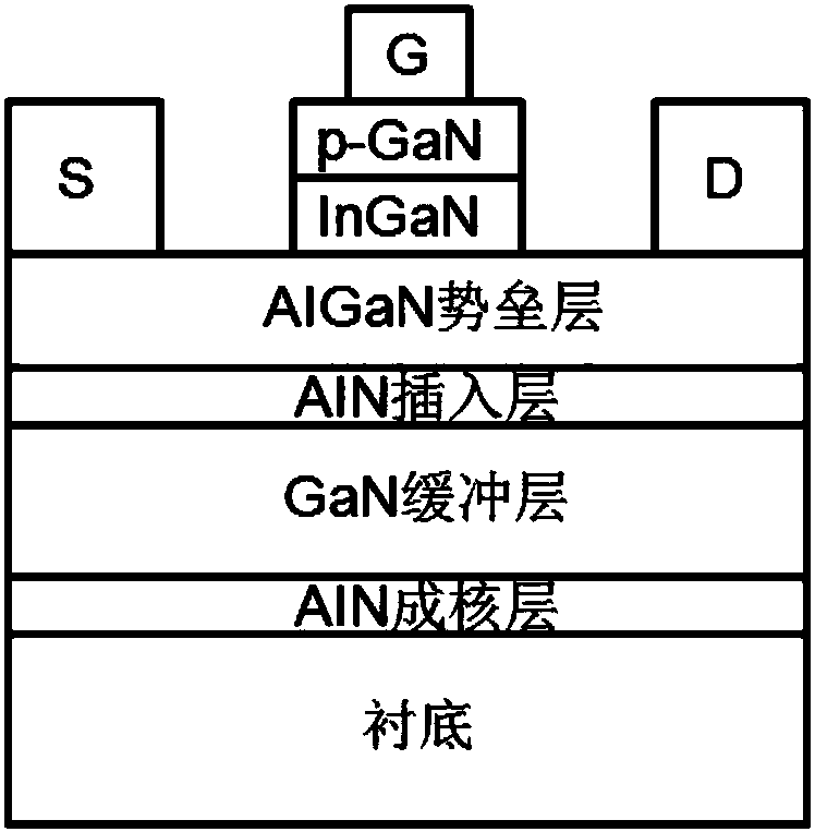
[0080] (1) GaN buffer layer, GaN channel layer ( That is, the first semiconductor), the AlGaN barrier layer (that is, the second semiconductor), and GaN as an oxidation self-stopping layer (that is, the third semiconductor), the structure of which is shown in Figure 6(a), where the GaN channel layer and the AlGaN potential The barrier layer forms a heterojunction, and a two-dimensional electron gas is formed in the heterojunction; then p-AlGaN (that is, the fourth semiconductor) is epitaxially grown on the oxidation self-stop layer GaN, and its structure is shown in Figure 6(b) Show;

[0081] (2) The source, drain region, and gate region on p-AlGaN (that is, the fourth semiconductor) by plasma-enhanced chemical vapor deposition PECVD or low-pressure chemical vapor deposition LPCVD (wherein the sour...

Embodiment 2

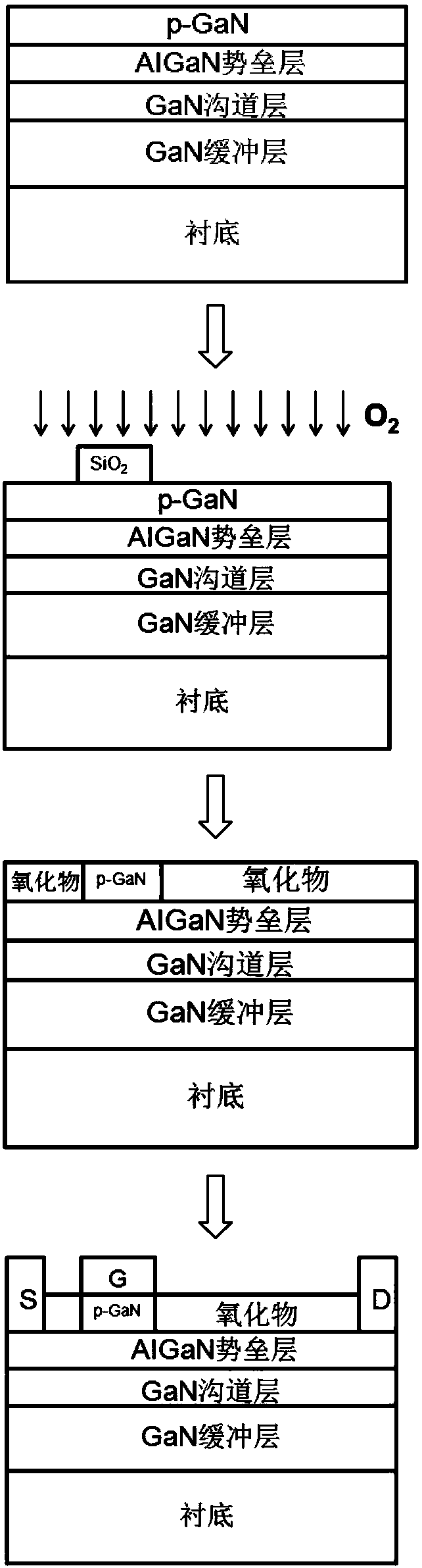
[0088] In this embodiment, the preparation method of the p-type gate enhancement transistor based on oxidation self-stop technology is basically the same as that of Embodiment 1 except for steps (2), (3) and (4). The steps in this embodiment (2): In the gate region of p-AlGaN (that is, the fourth semiconductor) (the material of the fourth semiconductor in this embodiment is p-AlGaN) by plasma-enhanced chemical vapor deposition PECVD or low-pressure chemical vapor deposition LPCVD (where the gate area or the area under the gate refers to the area corresponding to the gate) to grow SiO 2 or Si 3 N 4 Protective layer, the growth area can be determined by techniques such as photolithography and mask transfer, and its structure is as Figure 13 shown;

[0089] Step (3) is: with various oxidation methods such as oxidation method (including dry thermal oxidation, wet thermal oxidation, O plasma, annealing under oxygen-containing atmosphere, oxygen source can be O 2 , O 3 、H 2 O...


PUM


Abstract

The invention discloses a p-type gate enhanced transistor based on the oxidation self-stop technology and a preparation method thereof. The preparation method comprises the steps that a heterojunctionincluding a first semiconductor and a second semiconductor is provided, and two-dimensional electron gas is formed in the heterojunction; a third semiconductor and a fourth semiconductor are grown and formed on the heterojunction in turn; a mask film is arranged on the fourth semiconductor and the fourth semiconductor exposed out of the mask film is oxidized to form the oxide, and the oxidation reaction is enabled to self-atop when reaching the third semiconductor through the advantage that the oxidation rate of the fourth semiconductor is far greater than that of the third semiconductor under the same condition; and a source electrode, a drain electrode and a gate electrode are manufactured so that the gate electrode and the fourth semiconductor reserved in the area under the gate are enabled to be connected, wherein the fourth semiconductor reserved in the area under the gate is used for enabling the two-dimensional electron gas distributed in the area below the gate to be exhausted. The interface state produced by secondary epitaxy can be avoided, quasi-in-situ passivation is realized through formation of the oxide, the current collapse can be suppressed and the device performance can be enhanced.

Description

technical field [0001] The invention relates to an enhanced transistor, in particular to a p-type gate enhanced transistor based on oxidation self-stop technology and a preparation method thereof, belonging to the technical field of semiconductors. Background technique [0002] With the rapid development of the economy in today's era, people's awareness of environmental protection and resource conservation is becoming stronger and stronger, requiring lower and lower losses and higher efficiency in the process of energy conversion. In order to achieve this low loss and high efficiency Requirements, power electronic technology is needed to control energy conversion, and the core device of power conversion in power electronic system - power device, is used to effectively convert and control energy, thereby reducing energy consumption in the conversion process and realizing a high-efficiency conversion process . [0003] Power electronic devices are the core components of power...

Claims


Application Information

Patent Timeline
IPC IPC(8): H01L21/335H01L29/06H01L29/20H01L29/201H01L29/207H01L29/778
CPCH01L29/66462H01L29/0684H01L29/2003H01L29/201H01L29/207H01L29/7787
Inventor 孙驰何涛于国浩张宝顺
Owner SUZHOU INST OF NANO TECH & NANO BIONICS CHINESE ACEDEMY OF SCI
Why Eureka
Try Eureka