Optical detector of Van der Waals heterojunction based on two-dimensional indium selenide and black phosphorus and manufacturing thereof

A photodetector and indium selenide technology, applied in the field of photodetection, can solve the problems of low light absorption and luminescence efficiency, large dark current, limitation, etc., and achieve the effects of improving detection sensitivity, reducing response time, and reducing noise

Inactive Publication Date: 2018-08-24
QILU UNIV OF TECH
View PDF4 Cites 21 Cited by
  • Summary
  • Abstract
  • Description
  • Claims
  • Application Information

AI Technical Summary

Problems solved by technology

[0004] At present, the two-dimensional semiconductor van der Waals p-n heterojunction mainly faces the following problems: 1) The commonly used two-dimensional layered transition metal chalcogenides (TMDCs) materials are mainly n-type, and the electron mobility is low (electron effective Large mass), low light absorption and luminescence efficiency (single layer is direct band gap, multilayer is indirect band gap), etc., which lead to the failure of the electrical transport performance and photoelectric performance of the heterojunction, which limits its further optimization and improvement; 2) Although some p-type MoS 2 and WSe 2 Such as TMDCs can be achieved b

Method used


Image

  • Optical detector of Van der Waals heterojunction based on two-dimensional indium selenide and black phosphorus and manufacturing thereof
  • Optical detector of Van der Waals heterojunction based on two-dimensional indium selenide and black phosphorus and manufacturing thereof

Examples


Example Embodiment

[0044] Example 1

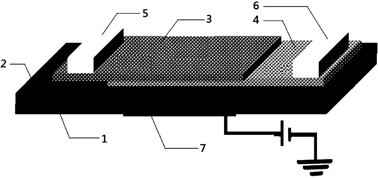
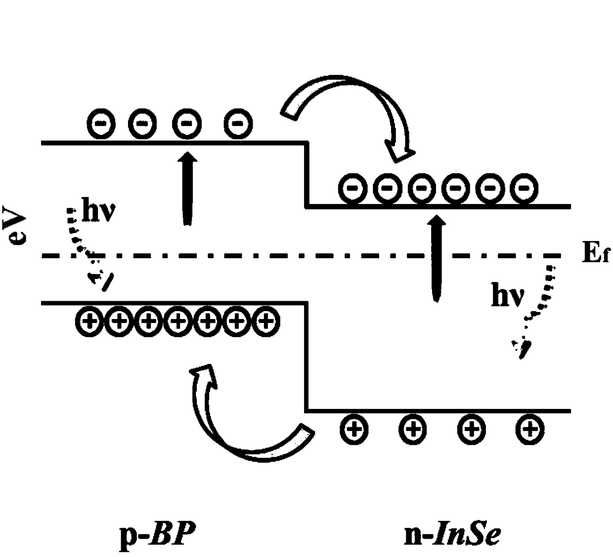
[0045] Such as figure 1 As shown, a photodetector based on a van der Waals heterojunction of two-dimensional indium selenide and black phosphorous includes a silicon substrate 1 and a silicon dioxide oxide layer 2 disposed on the silicon substrate 1. The silicon dioxide oxide layer 2 is provided with a p-type black phosphorous layer 4, the p-type black phosphorous layer 4 is provided with an n-type indium selenide layer 3, the p-type black phosphorous layer 4 and n-type selenium The indium layer 3 constitutes a van der Waals pn heterojunction;

[0046] The n-type indium selenide layer 3 is provided with a drain electrode, the p-type black phosphorous layer 4 is provided with a source electrode 6, and the silicon substrate 1 is provided on the side opposite to the silicon dioxide oxide layer 2 There is a gate electrode 7.

[0047] The thickness of the p-type black phosphorous layer 4 described in this embodiment is 10 nm, which is about 18 layers;

[0048] The th...


PUM

PropertyMeasurementUnit
Thicknessaaaaaaaaaa
Thicknessaaaaaaaaaa

Abstract

The invention relates to the optical detector of a Van der Waals heterojunction based on two-dimensional indium selenide and black phosphorus and manufacturing thereof. The optical detector comprisesa silicon substrate and a silicon dioxide oxide layer arranged on the silicon substrate. A p-type black phosphorus layer is arranged on the silicon dioxide oxide layer. An n-type indium selenide layeris arranged on the p-type black phosphorus layer. The p-type black phosphorus layer and the n-type indium selenide layer form a Van der Waals p-n heterojunction. A drain electrode is arranged on then-type indium selenide layer. A source electrode is arranged on the p-type black phosphorus layer. One surface of the silicon substrate, which is opposite to the silicon dioxide oxide layer, is provided with a gate electrode. In the invention, n-type indium selenide and p-type black phosphorus form the p-n heterojunction; through a built-in electric field at an interface, the rapid separating of electrons and hole carriers can be realized; a carrier composite probability is reduced and then the dark current of a device is deceased; and a detector noise can be reduced and a response speed is increased.

Description

technical field [0001] The invention relates to a photodetector based on a van der Waals heterojunction of two-dimensional n-type indium selenide and p-type black phosphorus and a preparation method thereof, which can realize low noise, high responsivity, fast response and wide spectrum The light detection belongs to the technical field of light detection. Background technique [0002] The ability of a single detector to achieve efficient light detection in a wide spectral range has important application value and has a wide range of applications in many fields, including optical communication, infrared imaging, remote sensing, environmental monitoring, spectral analysis, astronomical detection, etc. In the past, detectors that detect different wavelength bands can only be based on materials with different band gaps. For example, GaN is often used for ultraviolet light detection, Si for visible light detection, InGaAs for near-infrared light detection, and mid-infrared light...

Claims


Application Information

Patent Timeline
IPC IPC(8): H01L31/032H01L31/113H01L31/18
CPCH01L31/032H01L31/1136H01L31/18Y02P70/50
Inventor 李奎龙王文佳
Owner QILU UNIV OF TECH
Why Eureka
Try Eureka