Flexible antimony selenide thin film solar cell and preparation method thereof
A technology of solar cells and antimony selenide, which is applied to circuits, electrical components, photovoltaic power generation, etc., can solve the problems of damage to flexible substrates, difficulty in preparing high-quality thin films, poor crystallinity of thin films, etc., and achieves high energy conversion efficiency and preparation method. The effect of simple controllability and excellent bending properties
- Summary
- Abstract
- Description
- Claims
- Application Information
AI Technical Summary
Problems solved by technology
Method used
Image
Examples
preparation example Construction
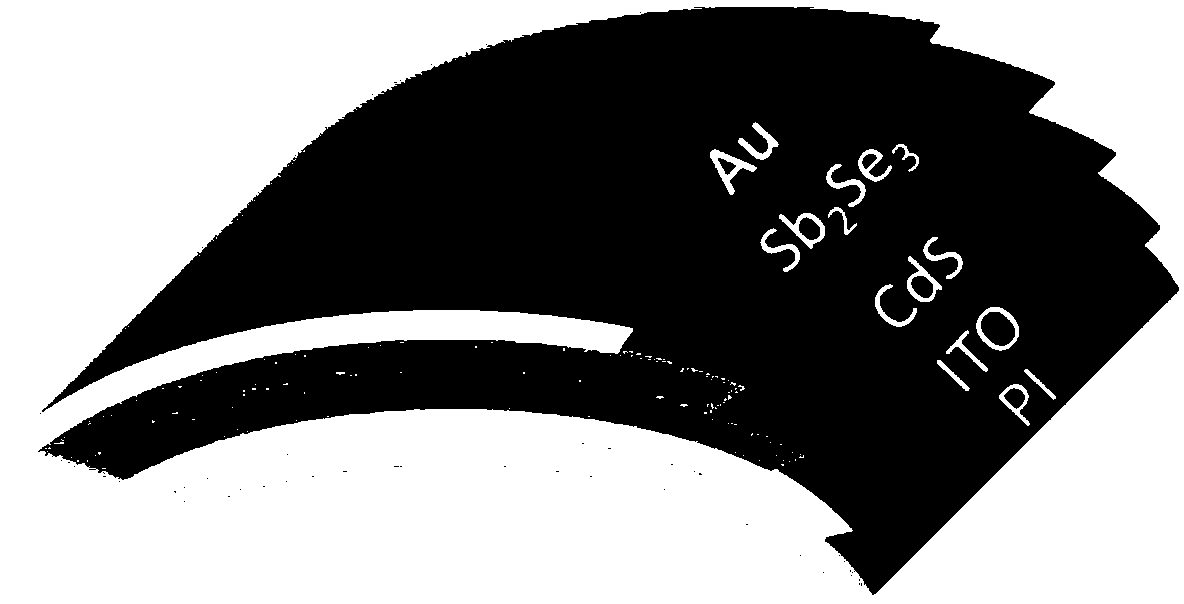
[0032] The flexible thin-film solar cell prepared by the present invention has a structural schematic diagram as figure 1 As shown, its specific structure is flexible substrate / ITO transparent conductive electrode / CdS film / Sb 2 Se 3 Film / Au electrode, the flexible substrate is polyimide, the thickness of the ITO transparent conductive electrode is 200nm-250nm, the thickness of the CdS film is 60nm-70nm, and the thickness of the antimony selenide film is 800nm- 1000nm, the thickness of the gold electrode is 80nm-100nm. The preparation method of the thin film solar cell comprises the following steps:
[0033] (1) With the rigid material as a support, the flexible substrate polyimide (PI) is placed on the rigid material glass, and the ITO transparent conductive electrode is deposited on the flexible substrate by magnetron sputtering. Polyimide (PI) flexible substrate has the characteristics of high transparency, high heat resistance and high acid and alkali resistance. Specif...
Embodiment 1
[0040] (1) Clean the glass-supported PI flexible substrate with deionized water, acetone, isopropanol, ethanol and deionized water in sequence for 10 minutes each, and then dry it with a nitrogen gun;
[0041] (2) Using magnetron sputtering to sputter ITO transparent conductive electrodes on the PI substrate, the thickness is 200nm, the transmittance is 78%, and the sheet resistance is 15Ωsq -1 ;
[0042] (3) Utilize the chemical water bath deposition method, the precursor is cadmium sulfate, ammonia water and thiourea, prepare CdS thin film on ITO conductive substrate, its thickness is 60nm;
[0043] (4) The antimony selenide thin film was prepared by vapor phase transfer deposition method, antimony selenide powder was used as the evaporation source, the vacuum degree was controlled at 3.0 Pa, the substrate temperature was 300 ° C, the temperature of the evaporation source was heated to 520 ° C, and the evaporation time was 3 min. The thickness of the antimony selenide film ...
Embodiment 2
[0047] (1) Clean the glass-supported PI flexible substrate with deionized water, acetone, isopropanol, ethanol and deionized water in sequence for 10 minutes each, and then dry it with a nitrogen gun;
[0048] (2) Use magnetron sputtering to sputter ITO transparent conductive electrodes on the PI substrate, the thickness is 250nm, the transmittance is 75%, and the sheet resistance is 10Ωsq -1 ;
[0049] (3) Using the chemical water bath deposition method, the precursor is cadmium sulfate, ammonia water and thiourea, and a CdS film is prepared on the ITO conductive substrate with a thickness of 70nm;
[0050] (4) The antimony selenide thin film was prepared by vapor phase transfer deposition method, antimony selenide powder was used as the evaporation source, the vacuum degree was controlled at 3.4 Pa, the substrate temperature was 350 ° C, the temperature of the evaporation source was heated to 540 ° C, and the evaporation time was 4 min. The thickness of the antimony selenid...
PUM
| Property | Measurement | Unit |
|---|---|---|
| Heat resistance temperature | aaaaa | aaaaa |
| Thickness | aaaaa | aaaaa |
| Thickness | aaaaa | aaaaa |
Abstract
Description
Claims
Application Information
 - R&D
- Intellectual Property
- Life Sciences
- Materials
- Tech Scout
- Unparalleled Data Quality
- Higher Quality Content
- 60% Fewer Hallucinations
Browse by: Latest US Patents, China's latest patents, Technical Efficacy Thesaurus, Application Domain, Technology Topic, Popular Technical Reports.
© 2025 PatSnap. All rights reserved.Legal|Privacy policy|Modern Slavery Act Transparency Statement|Sitemap|About US| Contact US: help@patsnap.com


