Si-based dual-faced solar cell structure based on local emitting electrode features
A double-sided solar cell and emitter technology, which is applied in the field of solar cells to achieve the effects of reducing recombination loss, increasing voltage, and increasing built-in potential
- Summary
- Abstract
- Description
- Claims
- Application Information
AI Technical Summary
Problems solved by technology
Method used
Image
Examples
Embodiment 1
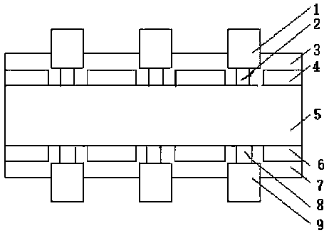
[0020] as attached figure 1 A Si-based double-sided solar cell structure with localized emitter characteristics is shown. The surface of the n-type crystalline silicon chip 5 adopts a pyramid textured structure with an average size of 3 microns in the regions where the passivation anti-reflection layer I 3 and the passivation anti-reflection layer II 7 are located. Both the electrode layer 2 and the heavily doped crystalline silicon field passivation layer 6 regions adopt a chemically polished surface structure (no texturing). The heavily doped n-type crystalline silicon field passivation layer I 4 has a thickness of 300nm; the heavily doped crystalline silicon field passivation layer 6 is n-type doped with a thickness of 5nm; the passivation anti-reflection layer II 7 is aluminum oxide + nitride Silicon composite film. The metal grid line I 1 and the metal grid line II 9 are nickel / copper / silver composite metal electrodes starting from the surface of the silicon wafer, occu...
Embodiment 2
[0023] as attached figure 1 A Si-based double-sided solar cell structure with localized emitter characteristics is shown. The surface of the n-type crystalline silicon chip 5 adopts a pyramid textured structure with an average size of 2 microns. The heavily doped n-type crystalline silicon field passivation layer I 4 has a thickness of 300nm; the heavily doped crystalline silicon field passivation layer 6 is n-type doped with a thickness of 5nm; the passivation anti-reflection layer II 7 is silicon oxide + nitride Silicon composite film. Metal grid lines I 1 and metal grid lines II 9 are pure silver electrodes, occupying 1.5% of the surface area of the silicon wafer. The groove width of the metal gate line I 1 and the metal gate line II 9 is 10 μm, and the groove width of the heavily doped p-type crystalline silicon emitter layer 2 and the n-type heavily doped crystalline silicon layer 8 is 8 μm.
[0024] Both surfaces of the solar cell structure have excellent light-inco...
PUM
 Abstract
Description
Claims
Application Information
 - R&D
- Intellectual Property
- Life Sciences
- Materials
- Tech Scout
- Unparalleled Data Quality
- Higher Quality Content
- 60% Fewer Hallucinations
Browse by: Latest US Patents, China's latest patents, Technical Efficacy Thesaurus, Application Domain, Technology Topic, Popular Technical Reports.
© 2025 PatSnap. All rights reserved.Legal|Privacy policy|Modern Slavery Act Transparency Statement|Sitemap|About US| Contact US: help@patsnap.com

