A kind of silicon-pedot: pss hybrid solar cell and preparation method thereof
A solar cell and hybrid technology, applied in the field of solar cells, can solve the problems of low photoelectric conversion efficiency, low electron mobility, loss, etc. of organic photovoltaic cells, and achieve the effects of enhancing built-in potential, increasing contact area, and improving work function
- Summary
- Abstract
- Description
- Claims
- Application Information
AI Technical Summary
Problems solved by technology
Method used
Image
Examples
preparation example Construction
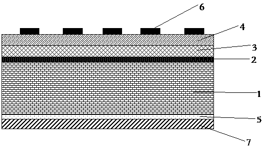
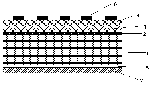
[0020] A method for preparing a silicon-PEDOT:PSS hybrid solar cell proposed in a specific embodiment of the present invention includes the following steps: (1) cleaning of the silicon substrate: ultrasonically cleaning the n-type silicon wafer in acetone, ethanol, and deionized water successively 10-30 minutes, and blow dry with nitrogen, then place the dried n-type silicon chip in a concentrated sulfuric acid / hydrogen peroxide mixed solution, heat treatment at 100-120°C for 40-60 minutes, and then rinse the n-type silicon chip with deionized water , and finally utilize hydrofluoric acid to remove the natural silicon oxide layer on the surface of the n-type silicon wafer; (2) surface passivation treatment of the silicon substrate: the n-type silicon wafer obtained in step 1 is blown dry with nitrogen, then immersed in saturated pentachloro In the chlorobenzene solution of phosphorus pentachloride, heat treatment at 110°C for 40-60 minutes, then the n-type silicon chip was take...
Embodiment 1
[0024] A kind of preparation method of silicon-PEDOT:PSS hybrid solar cell, comprises the following steps: (1) cleaning of silicon substrate: the n-type silicon chip is cleaned in acetone, ethanol, deionized water successively ultrasonic cleaning 20 minutes, and dry with nitrogen , then place the dried n-type silicon wafer in a concentrated sulfuric acid / hydrogen peroxide mixed solution, heat-treat it at 110°C for 50 minutes, then rinse the n-type silicon wafer with deionized water, and finally remove the n-type silicon wafer with hydrofluoric acid (2) surface passivation treatment of the silicon substrate: dry the n-type silicon wafer obtained in step 1 with nitrogen, then immerse it in a chlorobenzene solution saturated with phosphorus pentachloride, and heat treat it at 110°C 60 minutes, then the n-type silicon chip was taken out from the chlorobenzene solution of saturated phosphorus pentachloride and washed in chlorobenzene and tetrahydrofuran successively, and then the n-...
PUM
| Property | Measurement | Unit |
|---|---|---|
| length | aaaaa | aaaaa |
| diameter | aaaaa | aaaaa |
| thickness | aaaaa | aaaaa |
Abstract
Description
Claims
Application Information
 - R&D
- Intellectual Property
- Life Sciences
- Materials
- Tech Scout
- Unparalleled Data Quality
- Higher Quality Content
- 60% Fewer Hallucinations
Browse by: Latest US Patents, China's latest patents, Technical Efficacy Thesaurus, Application Domain, Technology Topic, Popular Technical Reports.
© 2025 PatSnap. All rights reserved.Legal|Privacy policy|Modern Slavery Act Transparency Statement|Sitemap|About US| Contact US: help@patsnap.com


